Agreed on all points.
The noise is already so low that there is little technical merit in making further improvements, while measurement inaccuracy, environmental noise, and self-noise make make it difficult to correlate the voltage regulator performance to the output.
Still, I'll see what adding 100 uF to C17 does. If there is an extra 3-6 dB left on the table it would be remiss of me to not take it. I should also take another look at bypassing R24.
"nicely melodic well detailed but natural sound"
Describes it perfectly. You wouldn't want to crank so hard on the reg that that presentation is lost for the sake of some better-looking FFT spectra. I'm definitely in the sweet spot already, but there may be a few last optimizations left undone.
Increasing C15 from 22 uF to 122 uF suppressed the two power harmonics visible in the FFT but did not alter the broadband noise.
(C15 is the first cap after the diodes.)
So we can say the broadband noise has nothing to do with noise on the voltage rail per se, it is generated internally either at the amplifier or regulator stages. The amplifier seems most likely given that the output noise does not show any attenuation effect of the CR filter stages, which the regulator noise would be expected to carry over at the output.
Attachments
Last edited:
Richard,
I did quick scans and searches of the thread and could not find the board dimensions. What are they?
Sorry if they are already listed and I just missed it!
TIA!
Greg in Mississippi
I did quick scans and searches of the thread and could not find the board dimensions. What are they?
Sorry if they are already listed and I just missed it!
TIA!
Greg in Mississippi
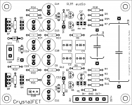
Each board is 80x100mm.
I should add that info to the BOM at least. Thanks for pointing that out.
I should add that info to the BOM at least. Thanks for pointing that out.
correction: C15 is now 22 uF + 220 uF = 242 uF not 122 uF.
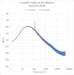
There are now no power line spikes, so we can look at what the broadband output noise translates to in terms of input-referred JFET noise.
This is a bit tricky since the second amplifier stage contributes most of the noise at high frequencies, while the first stage dominates at low frequencies. This is characteristic of a passive two stage RIAA design. What the plot below shows is the estimated noise characteristics of the first stage JFET amplifier.
I made the assumption that the high frequency noise of the second stage JFET is linear with frequency. Actually it has still has some residual curvature but this approximation does not affect the result much. I used the measured value, 50 dB, for the total circuit gain, and added 3 dB to the noise because, I remembered, audacity is averaging right and left channels so the uncorrelated noise is reduced 3 dB so I need to correct for that.
The long and short of it is the measured output noise is the value and shape predicted by the J113 datasheet. The roll off at low frequencies is due to the many bypass and coupling capacitors which are not accounted for here. The main point is there is no (or hardly any) additional noise from the power supply or external sources. It's just the JFET noise.
I still cannot explain why the noise decreased ~4-5 dB April->June however.
Attachments
Last edited:
I still cannot explain why the noise decreased ~4-5 dB April->June however.
Any voltage gain change in the DUT or in the test gear? Software drivers change? Some significant ambient temperature change? An erratic contact or solder joint stopped playing up? A noisy capacitor settled? RFI was possibly present then and now not?
I can't rule anything out at this point.
I'll have to go back to the original configuration and remeasure.
I'll have to go back to the original configuration and remeasure.
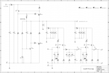
new 13c12 BOM for rev. 1.3c boards reflecting recent progress on the power supply front,
R15, 19 0R jumper (was 47.5 ohms)
R17, 24 22.1 ohms (was 33.2 ohms)
C15, C17 47 uF / 63 V (was 22 uF / 63 V)
Feel free to experiment making C15 even larger, but the BOM parts are chosen for what will fit in the existing board layout.
I'm still working on what the ideal capacitance value might be. 22 uF was a bit short, 220 uF is more than enough, looking at the earlier noise levels 100 uF is just right to knock the 120 Hz peak below the noise baseline. Doesn't matter terribly though if it's a bit higher or a bit lower.
/R
Attachments

Listening notes on changing the value of the input filter capacitor R15.
What the capacitor does:
It smooths out the rectified DC coming into the boards. It is the hardest working capacitor in the circuit, dealing with the largest charge/discharge currents.
What changing the value does:
The larger the capacitance, the lower the ripple voltage on the V++ going into the voltage regulator, and the lower the ripple voltage coming out of the regulator. At 242 uF the residual ripple drops below the broadband noise baseline, at 22 uF harmonics at 120 Hz and 240 Hz are present at about -90 dB or lower. However, the larger the capacitance, the greater the conductance angle: the transformer, diodes, and capacitor see a shorter, larger current spike many multiples higher than the average current draw of the circuit.
What I heard comparing 22 uF with 242 uF:
The larger value sounds more restrained, the smaller value sounds more relaxed. I prefer the smaller value, even though I couldn't hear quite as far into the recording. Having more focus on the foreground seems to me more natural. The big wall-of-sound presentation with the larger cap certainly had its moments though, but I found it too sterile overall.
Feel free to explore this, as I suspect there's a happy medium somewhere between those extremes. Relatively speaking the change is fairly obvious.
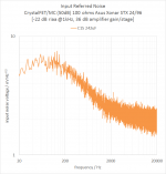
Since my 13c boards have gain and "boost" jumpers, I decided to see what they do.
This data should be treated as a qualitative result. The output noise is lower for the mm gain setting so the measurement system noise starts to creep in at high frequencies.
1. The boost function doesn't do anything for the noise, either for the baseline noise or the harmonics. There is a small change at very low frequencies, where the filter caps are no longer efficient. Actually the purpose of the boost is to lower the output impedance of the voltage regulator as well as lower the PSRR, so it may have an effect on bass response...
2. The mm switch decreases the gain by about 13-15 dB, as anticipated.
Attachments

Dear Richard,
yesterday I did a big mistake!
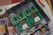
The preamp is 99% ready, I did 2 chassis version, the power supply is working wit 2X toroidal transformer 2X18V 50VA and I will post photos in the next days.
I connect the power supply to the boards and c15 cup in one channel is exploded because i did a wrong connection of the power supply.
Newer mind for the C15 as I'm waiting for new one with the value you have suggest in one of you early post, but in your experience, what other controls do I do in the circuit to see if any other component is blown?
Visually only this capacitor is broken, partly because I immediately turned off the power but if you need I will post a photo.
Thank you in advance for your help.
yesterday I did a big mistake!
The preamp is 99% ready, I did 2 chassis version, the power supply is working wit 2X toroidal transformer 2X18V 50VA and I will post photos in the next days.
I connect the power supply to the boards and c15 cup in one channel is exploded because i did a wrong connection of the power supply.
Newer mind for the C15 as I'm waiting for new one with the value you have suggest in one of you early post, but in your experience, what other controls do I do in the circuit to see if any other component is blown?
Visually only this capacitor is broken, partly because I immediately turned off the power but if you need I will post a photo.
Thank you in advance for your help.
That was unfortunate.
With a bit of luck though R14 (and sacrificially C15) should have protected the rest of the circuit from damage.
I would replace C15 and see if the voltages and currents look sensible, particularly the current through R14. If it is still 30-40 mA then it's probably all good. If it is much higher then there's a problem.
Check resistance of R14. If it still measures the listed value, you are probably ok. If that resistor is blown the damage likely extends further into the circuit.
Hi Richard,
I think I'm very lucky, I did measurement on R14 and seems Ok, also I did the R20 adjustment and easy went to 33V +-0,02V without any blown components.
Tomorrow I will try to connect it to my turntable.
Thank you for all your support!
I think I'm very lucky, I did measurement on R14 and seems Ok, also I did the R20 adjustment and easy went to 33V +-0,02V without any blown components.
Tomorrow I will try to connect it to my turntable.
Thank you for all your support!
Attachments
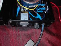
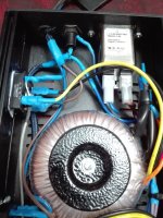

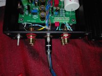
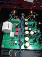
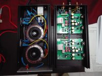
Looks very professional.
The phono stage chassis is a little small, and you've chosen to route the power cable right next to the input wires. That may be less than ideal...
The phono stage chassis is a little small, and you've chosen to route the power cable right next to the input wires. That may be less than ideal...
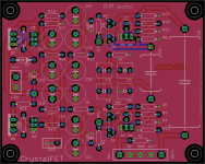
preview of next board revision, 14c
This is really just housekeeping, there are no major changes.
Schematic changes,
- boost switch is removed
- power supply emitter resistors removed
- 22 uF power supply caps increased to 220 uF
- power supply components renumbered
Board changes,
as above, and
- flat test pads replaced with wirepad test points, they are easier to use as probes don't slip so easily
- power supply layout compressed, moved left
- main circuit moved left, more space now for C8
- IN+ OUT+ labels moved to clear screw terminal package
If anyone has any requests, let me know. It'll be Monday before I send these to the fab.
Attachments
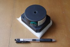
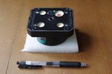
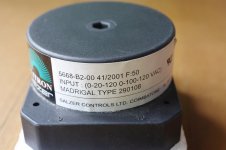
Speaking of housekeeping, I forgot to you show you guys the transformers I wrote about earlier.
The three brands on the label *Plitron*Salzer*Madrigal* should serve as a good indication of the quality we are dealing with here. For a 25VA part, they are enormous and extremely heavy. A steal at the asking price... but not the easiest to work with, as they of are designed to be fitted to a PCB rather than bolted directly to a chassis.
I'm thinking the best option is to knock up a quick layout and get some boards made at pcbway, just with the input and output connectivity and maybe the rectifier diodes. If anyone can provide the formal dimensions of the PC2 case these are potted in, it would be most helpful.
Attachments
Last edited:
rev 1.4e
- renumbered resistors
- small adjustments of component layout and silkscreen to improve label visibility
- renumbered resistors
- small adjustments of component layout and silkscreen to improve label visibility
Attachments
Last edited:
- Status
- Not open for further replies.
- Home
- Source & Line
- Analogue Source
- RJM Audio Crystal P jfet phono preamplifier | development thread