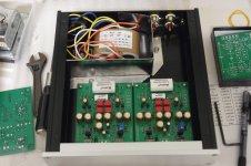
Speaking of which, here's another one of mine. This is 1.2a which I'm making for my Dad. He's got a DL-103 so it will be fixed gain, fixed load.
I needed it to have a convenient, small single chassis, which meant things got more crowded in there than I would like. There is a mu metal partition there enclosing the power supply. Hopefully that will be enough.
R-core is from ebay, China sourced. It has an electrostatic screen and the quality is quite reasonable.
Attachments
Quick note,
I've specified a 30 VAC secondary. If the load regulation of your transformer is unusually good, or the AC voltage in your area unusually low (110 of 110-120, or 220 or 220-240), the regulator may be just on the edge of dropping out.
The quick check: V++ should measure above 40 V.
If it is lower, adjust R20 to lower the V+, such that there is at least 5-6 V between V+ and V++. As long as TP2,3 are above 7 V it will be ok.
In extreme cases, you can increase the capacitance C15 or add capacitance to the power supply.
I would specify 2x18=36 VAC secondaries instead, but that risks, in extreme cases, being too much. 32 VAC would be ideal, while 30 VAC will work in just about all situations. Since 2x16 VAC transformers are not so common, I will leave the BOM as is for now.
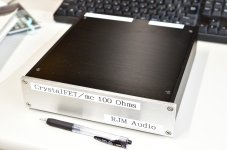
I finished my second. Pics for your reference.
I recommend a case that's 50% wider or deeper. Give yourself plenty of room to put the power supply well away from the boards. This one was way too cramped but it's what I had.
I recommend a case that's 50% wider or deeper. Give yourself plenty of room to put the power supply well away from the boards. This one was way too cramped but it's what I had.
Attachments
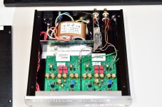
Managed to get some time to put this 1.2a into a box. Remote supply 2x15 secondaries, set to 35v on tp 1. Built with BOM parts, very clean😀.
I'm using a custom NWA cartridge output 0.1 mv so gain is a bit low. Suffering a problem with mains hum at present, maybe down to the small box.....I'll get to that later. It certainly holds some promise, thanks Richard.

Regards
Greg
I'm using a custom NWA cartridge output 0.1 mv so gain is a bit low. Suffering a problem with mains hum at present, maybe down to the small box.....I'll get to that later. It certainly holds some promise, thanks Richard.

Regards
Greg
Hi Greg, thanks for the report.
The cartridge output is a fair bit below what I was testing it with, but still the measured noise floor shows no harmonics above ~-100 dB so even with your cartridge the hum should be very very low.
You seem to have a couple of strange things going on.
First is the signal wires have what looks like a twisted pair both connected to IN+ and OUT+, and a separate (black) wire for the returns IN- OUT-. Actually you want IN+ and IN- connected as a tightly twisted pair, and OUT+ and OUT- also. Having a big loop of IN+ and IN- like that is going to cause a lot of noise pickup, especially as IN+ from the board runs over the power supply section of the other board.
Second, there seems to be a flying ground bus connecting GND on both boards to the ground lug on the chassis. This is fine, but there is also a rod running back to the third pin of the power connector. Actually, the CrystalFET chassis/GND does not connect to the power supply. There are only two connections, V++ and COM. I'd disconnect the flying bus from the power supply, just snip out that section with a pair of pliers.
See attached pdf for some diagrams.
Richard
Attachments
Last edited:
Hope it helps...
One other thought: what are your measured DC voltages V++ and TP1?
(TP1 should be about 33-34 V, but how about V++?)
/R
One other thought: what are your measured DC voltages V++ and TP1?
(TP1 should be about 33-34 V, but how about V++?)
/R
Hi Richard,
V++ 44v dc rectified from 2 x15v secondaries
TP1 34v dc
I'll find a larger case and spread things out more and get the signal away from the power on the board..
Regards
Greg
V++ 44v dc rectified from 2 x15v secondaries
TP1 34v dc
An externally hosted image should be here but it was not working when we last tested it.
I'll find a larger case and spread things out more and get the signal away from the power on the board..
Regards
Greg
Last edited:
It looks good now, so far as I can tell from eye-balling it from here.
Did those changes not help at all? The power supply is already external. While there is some concern about the input signal wires being close to the regulation part of the boards, I wouldn't expect a large pickup, and I would expect it to be significantly improved by fixing the twisted pair as you have done.
I'm not convinced the problem is the crowding in the case, in other words.
1. You have no load resistor on the RCA input jacks, so I assume you have replaced R1 with the value appropriate for your cartridge.
2. Is the hum 60 Hz or 120 Hz? Worse or better when the phono leads are unplugged from the input? Worse or better when the TT ground is disconnected from the ground lug? How about with just one channel powered up?
3. Is there anything that seems to influence the magnitude of the hum?
1) load is 100 ohm
2) No difference for phono leads in or out or TT ground.
3) pre-amp volume settings
On the up side the reproduction on very low volume levels is really very good 😀
Regards
Greg
2) No difference for phono leads in or out or TT ground.
3) pre-amp volume settings
On the up side the reproduction on very low volume levels is really very good 😀
Regards
Greg
Last edited:
100uf in the power supply has reduced the noise. Putting the 'scope on the board input showed significant noise, cleaning that up should improve matters. I'll do a bit more on the supply.
From what you have told me I can infer three possible causes,
1. Systemic noise coupling of the power supply ripple into the signal at the board level. (unlikely since mine test fine)
2. Incorrect configuration of the voltage regulator and filtering elements.
(possible but unlikely since you can adjust to the correct output voltage without any problem, indicating that's its basically working. I assume here you have built it according to the BOM without modification)
3. Regulator running out of spec. (my gut feeling says this is the problem)
The CrystalFET uses a shunt regulator. It works by using CCS Q7 to send a fixed current to the phono stage and shunt element (Q8), and adjusting the current through the shunt element to keep the V+ voltage constant. The shunt current + the circuit current = the total current provided by Q7. If the circuit current draw is equal or greater to the total, there is no current left over to shunt and the regulator stops working.
The total current supply is controlled by R17. You can check the shunt current by measuring the voltage across R24 (I = V/R). If the shunt current is less than 5 mA you should decrease R17 until it's about 10 mA.
I can check for you against my simulation if you can provide me with a few key circuit values. Sometimes it might just be a simple matter of adjusting R20 to lower V+ a shade which lowers the circuit current and brings the system back into working shunt range. Last resort decreasing R17 will certainly kick it up into the working range.
PS. Since the noise is independent of the input connection, you could bring the phono stage over to a computer and record the output signal. An FFT of this data (using Audacity or Rightmark) would give us a quantitative look at the situation.
Last edited:
Hi Richard, I have checked the boards, there are no errors I can see regarding construction. The parts values are as supplied in the BOM you mailed me with the boards, (caps and resistors measured prior to fitting, I measured 200 J113 to get close tolerance parts) all parts from Farnell so should be no fakes, although the manufacturers may be different.
The shunt current across r24 is 8mA.
What other measurements do you need for further analysis?
I'll get the audacity plot sorted when I can (input will be through M-Audio delta 192 ), what length of sample would give you enough data ?
Regards
Greg
The shunt current across r24 is 8mA.
What other measurements do you need for further analysis?
I'll get the audacity plot sorted when I can (input will be through M-Audio delta 192 ), what length of sample would give you enough data ?
Regards
Greg
Last edited:
Thanks Greg! 8 mA indicates the shunt is all working like it's supposed to, so I'll wait until the FFT to comment further.
Sample length only needs to be a fraction of a second, a couple of seconds of data is more than enough.
Sample length only needs to be a fraction of a second, a couple of seconds of data is more than enough.
FET Matching
Hello
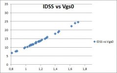
I started matching the J113 Fets I had at hand (Fairchild from Mouser ordered 2015). Most of them have Vgs0 arround 1-1.2V with IDSS arround 10-15. Only a few are higher at 1.4-1.6V Vgs0. Closest matches can be found at Vgs0 = 1.2V and gm@1mA=6.2 (+/-0.01).
I measured 40 out of ~100 and getting tired of the matching process so I'll start building my 1.02a Version now 😱
I'll do some measurements and post my results here. I'll also compare to the High Octane and some other phono-pre's.
kind regards, Daniel
Hello
I started matching the J113 Fets I had at hand (Fairchild from Mouser ordered 2015). Most of them have Vgs0 arround 1-1.2V with IDSS arround 10-15. Only a few are higher at 1.4-1.6V Vgs0. Closest matches can be found at Vgs0 = 1.2V and gm@1mA=6.2 (+/-0.01).
I measured 40 out of ~100 and getting tired of the matching process so I'll start building my 1.02a Version now 😱
I'll do some measurements and post my results here. I'll also compare to the High Octane and some other phono-pre's.
kind regards, Daniel
Attachments

I feel your pain. I measured 200 of the dang things.
Yours seem to be measuring a little lighter than mine, 1.2 V rather than the 1.4 V typical I got. That's actually good, in the sense that you want slightly lower values if possible to maximize the voltage gain of the amplifier stages. The follower is non-critical.
Match two pairs from around Vgs0 = 1.2 V and you'll be on your way. Drain resistors R2,8 will need to be about 24-26 kohms I expect.
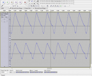
I'm at a loss to explain this one.
50 Hz sine wave with a chunk lopped off part of the peak. ~10 mV rms at the output of the CrystalFET. Such a waveform does not normally exist in the CrystalFET circuit, at any magnitude. If I had to guess : noise from a high current half-wave rectifier power supply (something big and nasty, not audio) polluting the AC line and earth and injected into the CrystalFET via some a ground loop.
50 Hz sine wave with a chunk lopped off part of the peak. ~10 mV rms at the output of the CrystalFET. Such a waveform does not normally exist in the CrystalFET circuit, at any magnitude. If I had to guess : noise from a high current half-wave rectifier power supply (something big and nasty, not audio) polluting the AC line and earth and injected into the CrystalFET via some a ground loop.
Attachments

Last edited:
- Status
- Not open for further replies.
- Home
- Source & Line
- Analogue Source
- RJM Audio Crystal P jfet phono preamplifier | development thread