I'm doing better with the Siliconix J113 which arrived from the UK.
These are properly in spec, V_gs0 1.5 V and I_dss 35 mA, close to the center of the datasheet values. The beta is about 15 mA/V^2.
That's a quick estimate. Although higher current than ideal (the five parts I checked are grade C to F2 on my little chart) the circuit is workable at 35 V and finding well matched parts should not be a problem.
Attachments
Last edited:
More fun and games with Chinese-sourced jfets via eBay, this time with parts marked Fairchild 2N5484.
The good news is most of them seem to be genuine or at least to-datasheet-spec, with V_gs0 1.3 and I_dss 2.1 mA and a usefully high beta of 1.3 mA/V^2.
But then there's an oddball weirdo in the mix, which measured like a J111. Just to keep you on your toes I guess.
Moral of the story: do not buy semiconductors off ebay from from China-based sellers unless you are prepared to a full screening to properly identify what actually shows up.
Attachments
So, after consideration, I have come down to two options:
1. J113 running at 5 mA I_ds from a 35 V supply. 32 dB gain, no bypass caps. [Adding bypass caps, the circuit makes 55 dB for MC use.]
(advantages: high transconductance, low distortion, MC/MM dual use)
2. 2N5484 running at 1 mA I_ds from a 25 V supply. 32 dB gain, no bypass caps or 40 dB with bypass caps).
(advantages: low current, optimized operating point, 40 dB MM output option with bypass caps)
2b. Use 2N5484 as the amplifier, and a J113 or similar for the follower)
I am favoring option 1, though 2b seems to have merit also. It comes down to this: for a given operating current, say 3 mA, is a jfet with higher or lower saturation current more desirable?
Normally it's a non-issue, as higher saturation current means more transconductance (lower output impedance) and lower saturation current means higher gains but in this instance the fact that the J113 can be used at 35 V while the 2N5484 is limited to 25 V, together with the high beta value of the J113 and the degenerative feedback of the source resistors, means that the gain has a certain degree of overlap.
My gut feeling is that if it the gain specifications can be met, then the higher transconductance part is desirable. The concern of course is the existance is some hidden "gotcha" that I haven't considered.
Attachments
Last edited:
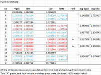
Matching results from 20 2N5484,
4 fakes.
2 "A" grade matched pairs (beta match <3%, beta above 1mA/V^2)
4 normal matched pairs
4 unmatched
* match efficiency 60% (75% if you don't count the fakes) I can build a nice CrystalFET from 20 jfets, obtained off ebay for <$5.
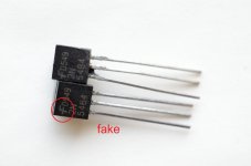
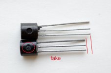
** the fakes are different physically from the actual Fairchild parts. The leads are slightly shorter, the font and logo print less sharp, and there is an "x" mark in the mold stamp on the rear of the package.
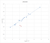
*** with a couple of exceptions the plot of I_dss vs. (V_gs0)^2 is a straight line. That means for a given model of jfet if you know the pinch off voltage you can imply the saturation current, and vice versa, with reasonable confidence. In other words It means you can bin (match) by pinch off voltage though for best results the two-point method is still recommended.
**** "size" is my own figure of merit, I_dss x (V_gs0)^2. Basically how far up the line in the plot below. jfets with the same size will tend to bias to the same operating point with a common set of resistor values, obviously important when matching between channels, together with the gain, which is defined by the beta. "Size" allows for a little more compensation that matching strictly to both V_gs0 and I_dss individually, and is more reliable than just V_gs0 alone.
***** The 2N5457 I received from anoter ebay seller appear to be 100% fakes. All short leads, same general appearance as the fake 2N5484, but with a "II" mark instead of the "X" mark in the mold release hole.
4 fakes.
2 "A" grade matched pairs (beta match <3%, beta above 1mA/V^2)
4 normal matched pairs
4 unmatched
* match efficiency 60% (75% if you don't count the fakes) I can build a nice CrystalFET from 20 jfets, obtained off ebay for <$5.
** the fakes are different physically from the actual Fairchild parts. The leads are slightly shorter, the font and logo print less sharp, and there is an "x" mark in the mold stamp on the rear of the package.
*** with a couple of exceptions the plot of I_dss vs. (V_gs0)^2 is a straight line. That means for a given model of jfet if you know the pinch off voltage you can imply the saturation current, and vice versa, with reasonable confidence. In other words It means you can bin (match) by pinch off voltage though for best results the two-point method is still recommended.
**** "size" is my own figure of merit, I_dss x (V_gs0)^2. Basically how far up the line in the plot below. jfets with the same size will tend to bias to the same operating point with a common set of resistor values, obviously important when matching between channels, together with the gain, which is defined by the beta. "Size" allows for a little more compensation that matching strictly to both V_gs0 and I_dss individually, and is more reliable than just V_gs0 alone.
***** The 2N5457 I received from anoter ebay seller appear to be 100% fakes. All short leads, same general appearance as the fake 2N5484, but with a "II" mark instead of the "X" mark in the mold release hole.
Attachments
Last edited:
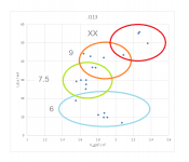
Matching report for 20 Siliconix J113s.
The scatter of these jfets is different than the Fairchild ones I've looked at. The V_gs0 traces an arc as the saturation current increases, so minimum pinch off voltages are obtained for the mid-range saturation currents.
That actually makes them easy to deal with from the point of view of the CrystalFET circuit since the range of pinch off voltages is very narrow, just 1.25 V to 1.55 V. All of the 20 components measured would be suitable, though only 12 were matched, with three of those pairs found to be "A" (amplifier) grade.
The circuit gain is about 32 dB, while adding bypass capacitors would allow the circuit to be used as a 58 dB MC stage.
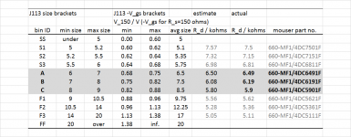
I have graded the J113 into four bins "6", "7.5", "9", and "XX". The drain resistor R2,8 will be slightly different for each bin, but no other components will need to be changed.
The scatter of these jfets is different than the Fairchild ones I've looked at. The V_gs0 traces an arc as the saturation current increases, so minimum pinch off voltages are obtained for the mid-range saturation currents.
That actually makes them easy to deal with from the point of view of the CrystalFET circuit since the range of pinch off voltages is very narrow, just 1.25 V to 1.55 V. All of the 20 components measured would be suitable, though only 12 were matched, with three of those pairs found to be "A" (amplifier) grade.
The circuit gain is about 32 dB, while adding bypass capacitors would allow the circuit to be used as a 58 dB MC stage.
I have graded the J113 into four bins "6", "7.5", "9", and "XX". The drain resistor R2,8 will be slightly different for each bin, but no other components will need to be changed.
Attachments
Last edited:
LTSpice is not reality.
Patrick
I never could get the level 3 model to work in LTSPICE (and now it is banned from ADI computers for obvious legal reasons). The level 1 model is a joke for anything more than basic functionality.
I would suggest you use a dual footprint for the jfets, use a SOT-23/TO-92 footprint. It leaves you with way more options rather than resorting to Ebay for your sources, unless you only plan on making a few of them.
Gain trim pots to balance the channels.
Gain trim pots to balance the channels.
I am sure LTC would appreciate your input for improving the functionality 🙂I never could get the level 3 model to work in LTSPICE
LTSpice is just a big calculator. For that purpose it is very useful.
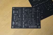
Latest circuit revision attached.
(I considered using trim pots on the source to adjust the bias, but with well-matched jfets in self-biasing arrangement I figured it wouldn't be needed. I'm using "tube logic" in a number of areas with respect to the jfets here, we'll see how it goes.)
Latest circuit revision attached.
(I considered using trim pots on the source to adjust the bias, but with well-matched jfets in self-biasing arrangement I figured it wouldn't be needed. I'm using "tube logic" in a number of areas with respect to the jfets here, we'll see how it goes.)
Attachments
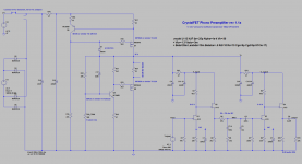
BOM updated to 1.1a4.
Several small changes to the components.
Calculation worksheets completely revised.
For the base MM configuration if you can obtain matched pairs of J113 with "size" = V_gs0 x sqrt(I_dss) between 6 and 9, you can use the BOM values as-is, R2,R8 = 6.19 kohms. Provision is made, however, for adjusting R2,8 precisely to any given J113 size.
The MC configuration is more of a side project. Yes, by adding bypass caps C1,7 to the source resistors gain shoots up to 58 dB, but the loss of all that degenerative feedback means the phono stage gain is ten times more sensitive to the JFET matching. R5 should be increased to 33k and the appropriate cartridge loading taken care of at the input.
Attachments
[BETA TESTERS]
(shipping is included)
1 pair CrystalFET boards $20.
1 pair CrystalFET boards + full set matched J113 JFETs only: $35.
1 CrystalFET beta kit (MM config, boards and all parts to complete boards except C6 and C8): $75. [four kits available]
(shipping is included)
1 pair CrystalFET boards $20.
1 pair CrystalFET boards + full set matched J113 JFETs only: $35.
1 CrystalFET beta kit (MM config, boards and all parts to complete boards except C6 and C8): $75. [four kits available]
Attachments
Hi, I would like to build the complete kit, but I live in Italy and... are you shure the shipping cost are included? 😉
Also, what means be a beta tester, I'm asking this becouse I dont have any special instrument but a normal tester.
Thank you
Sergio
Inviato dal mio PLK-L01 utilizzando Tapatalk
Also, what means be a beta tester, I'm asking this becouse I dont have any special instrument but a normal tester.
Thank you
Sergio
Inviato dal mio PLK-L01 utilizzando Tapatalk
The prices above are discounted about 50% since this is a beta run, but it's enough to more-or-less cover components, fabrication, shipping and Paypal fees.
To be a beta tester ... means at a minimum using a multimeter to check circuit voltages, it means less polished written instruction, and, let's say, it means being able to make changes afterwards by substituting some resistors.
To be a beta tester ... means at a minimum using a multimeter to check circuit voltages, it means less polished written instruction, and, let's say, it means being able to make changes afterwards by substituting some resistors.
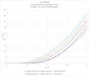
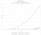
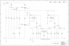
Latest BOM, rev. 1.1a6.
Added mouser part numbers for C6 and C8, though recommend upgrading to Multicap PPMFX (partsconnexion) or similar.
Capacitor max body length for C6 is 20 mm, 50 mm for C8. Axial type. There is room to manage even larger capacitors, or use long leaded radial types like 715P, but it won't look as pretty. Wima box types won't fit.
Changed the lookup table for R2,8 so the chosen resistance values step evenly.
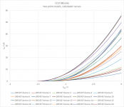
Added most recent simulated response curves. These are LTSpice results for the whole circuit including all the coupling caps.
Added mouser part numbers for C6 and C8, though recommend upgrading to Multicap PPMFX (partsconnexion) or similar.
Capacitor max body length for C6 is 20 mm, 50 mm for C8. Axial type. There is room to manage even larger capacitors, or use long leaded radial types like 715P, but it won't look as pretty. Wima box types won't fit.
Changed the lookup table for R2,8 so the chosen resistance values step evenly.
Added most recent simulated response curves. These are LTSpice results for the whole circuit including all the coupling caps.
Attachments
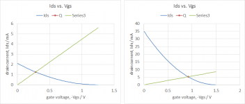
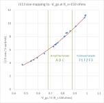
While at first glance the I_dss and V_gs0 values for the J113 appear to be scattered at random, there is in fact a very close correlation.
That is, there is only a very narrow range of possible V_gs0 values for a given value of I_dss. It is easy enough to link the two parameters empirically, I use a measure called "size" defined as [V_gs0 x sqrt(I_dss)]. It turns out that pretty much every other parameter can be expressed as continuous function of size, including the gate-source test voltage for source resistance 150 ohms. (see attached plot)
So this quick voltage measurement (with gate grounded and R_source 150 ohms) can be used to bin the J113 jfets according to the table. A B C grades are used for the amplifier, while F grades are used for the follower. S grades are not useful in the CrystalFET circuit and are kept for other applications.
The circuit gain for jfets of any given grade ("B", for example) should be well within 0.5 dB (MM version), but of course this can be improved by selecting matched pairs within a grade.
Matching within a size bin 0.2 wide is more than sufficient. In terms of the voltage measurement at R_s 150 ohms, this means matching within 15 mV. With just 20 components I could obtain 3 matched pairs of (A,B,C) grade jfets, and enough F grade parts to complete the circuit.
This means: if you are planning to build this and use your own parts, you'll need to buy at least 15 J113s, but no more than 25 should be necessary.
Attachments
a7 BOM
R11 changed from 22k to 47k. 22k was a mistake, I'd set that in the simulation to model the actual load and forgot to change it back to a nominal value for actual circuit.
R11 can be any value between 47k and 100k. The effective load (R11||actual loading) should be about 20-30k for best results.
R11 changed from 22k to 47k. 22k was a mistake, I'd set that in the simulation to model the actual load and forgot to change it back to a nominal value for actual circuit.
R11 can be any value between 47k and 100k. The effective load (R11||actual loading) should be about 20-30k for best results.
Attachments
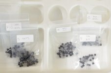
Churned through 200 J113 jfets to sort into bins.
approx. part count:
S 50 (unused, size <6)
A 43 (amp grade, size 6-7)
B 19 (amp grade, size 7-8)
C 28 (amp grade, size 8-9)
F 60 (follower grade F1,2 size 9-14)
There is a "double hump" in the distribution, so more A and C than B, but 45% of the total were "amplifier grade" and another 30% were "follower grade". That's a pretty good harvest. The balance of followers can be made up from poorly matched jfets from the amplifier grades.
Attachments
Last edited:
I would the psu build without the separate R-C at the two stages and without, if, bridging, different caps. And NO channel separate psus. That does rip the homogenity, the sound, the clearness (May be, many more caps, ex. 30 x 220 uF, or 50 x 1 mF - same, at ONE circuit - do open the performance very much). The most do separate, cause they simply copy or have multiwayspeakers,-)
There is a chance to get a superb phonoamp, with reduced/less influence, differences of components: transes, resistors, caps, solders, pcb... Better: revise poweramps, speakers, rooms, all equipment.
There is a chance to get a superb phonoamp, with reduced/less influence, differences of components: transes, resistors, caps, solders, pcb... Better: revise poweramps, speakers, rooms, all equipment.
For the record I have two concerns with this whole thing,
1. Gain. Only about 31-32 dB. (52-54 dB MC) Touch and go but there's not much I can do about it.
2. Matching jfets for MC. No degenerative feedback, so matching needs to be about 5x closer than the MM version. Where size difference 0.2 is sufficient for MM, for MC the tolerances tighten to 0.01. (for <0.1 dB channel imbalance)
That's pretty much it for the practical operation. The rest comes down to how it will sound.
@cumbb As far as I can tell we are in agreement, more-or-less. I'm not thrilled with the RC stages in the power supply, but the ripple would otherwise be too large. It is easy to remove the RC filter stage from the circuit by shorting over the resistors, however, so experiments along that line are possible down the road.
- Status
- Not open for further replies.
- Home
- Source & Line
- Analogue Source
- RJM Audio Crystal P jfet phono preamplifier | development thread