I will try to increase the value of the SMD resistor I put in parallel with the big inductive ones.
aaand... with 4R7 in parallel, the magic disappears and the peaks come back. Not enough damping. So with this particular circuit, layout, and resistor inductance it has to be 1 ohm...
I was just about to solder 4.7 ohms to my 0.18 ohm emitter resistors for testing in the amplifier.
It's good that you got ahead of me so that I didn't do it.
It's good that you got ahead of me so that I didn't do it.
I think the best value depends on the inductance of the wirewound resistors which is not specified in the resistors datasheet, so it would be a shot in the dark to attempt that as a tweak.
But I agree with anatech that non inductive resistors solve the problem, either the expensive flat ones, or you can DIY a non inductive resistor by cutting a small piece of blank copper clad pcb, cutting the copper in two halves, and soldering enough SMD resistors on it...
I was curious, so I made one with a bit of cardboard and some copper tape.

It's a 0R15 resistor with an inductance of about 2nH. Mounted vertically it could even dissipate a few watts ; the copper tape makes a nice heat sink, it burned my fingers while I held it by the edge soldering it. Could make tiny PCBs like that from a cheap fab like jlcpcb...
But I agree with anatech that non inductive resistors solve the problem, either the expensive flat ones, or you can DIY a non inductive resistor by cutting a small piece of blank copper clad pcb, cutting the copper in two halves, and soldering enough SMD resistors on it...
I was curious, so I made one with a bit of cardboard and some copper tape.
It's a 0R15 resistor with an inductance of about 2nH. Mounted vertically it could even dissipate a few watts ; the copper tape makes a nice heat sink, it burned my fingers while I held it by the edge soldering it. Could make tiny PCBs like that from a cheap fab like jlcpcb...
Last edited:
CORRECTION
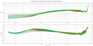
I wanted to put in the lateral FETs this morning, and then I saw one of the 4R7 resistors was not properly soldered. This means the previous HF test with 4R7 is absolutely wrong. Since the SMD resistor did not make contact, it is not surprising that it gave the same result as the test without the SMD resistor! Well this mistake still gives information: with only the inductive emitter resistors, the peak also manifests in the output impedance, not just in the input/output transfer function, which is logical.
So I fixed the solder joint and re-ran the test : it gave a very smooth spectrum.
I ran it again with 15R resistors in parallel with the inductive 0R15 resistors : again, no problem at all.
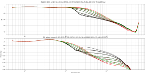
Attached is output impedance with 4R7 and 15R resistors. There is a small soft peak in the region of interest, which hints that values above 15R would not provide enough damping.
Also a test without the output Zobel network (100n+4R7). This shows no gremlins, so messing with the emitter resistors could perhaps allow to get rid of the Zobel network.
So there seems to be quite a lot of flexibility in the choice of the resistor value.
I wanted to put in the lateral FETs this morning, and then I saw one of the 4R7 resistors was not properly soldered. This means the previous HF test with 4R7 is absolutely wrong. Since the SMD resistor did not make contact, it is not surprising that it gave the same result as the test without the SMD resistor! Well this mistake still gives information: with only the inductive emitter resistors, the peak also manifests in the output impedance, not just in the input/output transfer function, which is logical.
So I fixed the solder joint and re-ran the test : it gave a very smooth spectrum.
I ran it again with 15R resistors in parallel with the inductive 0R15 resistors : again, no problem at all.
Attached is output impedance with 4R7 and 15R resistors. There is a small soft peak in the region of interest, which hints that values above 15R would not provide enough damping.
Also a test without the output Zobel network (100n+4R7). This shows no gremlins, so messing with the emitter resistors could perhaps allow to get rid of the Zobel network.
So there seems to be quite a lot of flexibility in the choice of the resistor value.
Attachments
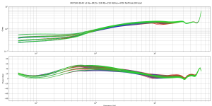
Time for laterals.
While the input capacitance of the N and P channel IRFP FETs was well matched, this is not the case for the laterals. The P-ch capacitances increases much more as it loses headroom.

Since it doesn't have higher gm to compensate, this is visible on the fT plot on the left too.

So, the network analyzer gives two series of distinct curves. Green color shows when both FETs have ample voltage headroom, and there are two distinct sets of green curves, depending on which FET is ON (which one is on depends on polarity of output current, not output voltage).

Previously I had put a ferrite bead on the source, without these FETs would oscillate. In this case I have lifted the pin of the FET off the PCB and soldered a 130R SMD gate resistor right there. It seems to be as effective as the ferrite bead at preventing oscillation.
I will do another run with the ferrite bead then compare the laterals and IRFPs.
While the input capacitance of the N and P channel IRFP FETs was well matched, this is not the case for the laterals. The P-ch capacitances increases much more as it loses headroom.
Since it doesn't have higher gm to compensate, this is visible on the fT plot on the left too.
So, the network analyzer gives two series of distinct curves. Green color shows when both FETs have ample voltage headroom, and there are two distinct sets of green curves, depending on which FET is ON (which one is on depends on polarity of output current, not output voltage).
Previously I had put a ferrite bead on the source, without these FETs would oscillate. In this case I have lifted the pin of the FET off the PCB and soldered a 130R SMD gate resistor right there. It seems to be as effective as the ferrite bead at preventing oscillation.
I will do another run with the ferrite bead then compare the laterals and IRFPs.
The few times I tried it, LTSPICE simulation gave a quite reasonable estimate of the "Cartesian" input impedance of a follower: Re(Zin) + j*Im(Zin). When LTSPICE says the real part of Zin is negative-ABC, I installed a base stopper resistor whose value is 2*ABC and presto, oscillation ceased. Who knows, perhaps 130R is waaaay bigger than necessary; LTSPICE might offer a helpful perspective.

V7 is set to 1V AC (in blue, representing distortion as a voltage added by the output stage to the VAS output node). Since the amp uses second order compensation, at 1kHz it is reduced by a huge factor of 220k. To get the same output distortion by injecting a current into the VAS node, current source I3 would need to be set to AC 50µA (red). So to compare the influence of voltage and input current nonlinearities in this output stage, a source impedance of 20k should be used (at 1kHz). That corresponds more or less to the open loop output impedance of this VAS.
But what's the open loop output impedance of the VAS at 20kHz? Likely less than 1k, which is close to a voltage source from the point of view of most OS's. At the top end the global feedback is least able to linearize the OS, but this is where the OS is driven with the lowest impedance.
So in my opinion the wing-spread diagrams of voltage gain are more pertinent to distortion produced by an output stage in a real amplifier - after all a good amp only lightly loads the VAS anyway to reduce VAS distortion due to varying load impedance.
Thus throwing extra current gain into the OS reduces the effect of non linear current gain in the OS, leaving only the voltage gain non-linearity from the OS as the main offender the global feedback has to deal with at higher frequencies.
I did a bit of spice experimentation showing a typical VAS with 100pF Cdom having at output impedance of 22k at 500Hz, 3.5k at 2.5kHz and 700 ohms at 12.5kHz. An OS might be in the 10k--20k ohm region for its input impedance.
Another way to characterise OS distortion is in a complete amp circuit, but you assume the output is linear, and monitor the VAS output node to measure OS distortion (well, its inverse distortion in fact). You assume the OS is dominant source of distortion in the loop.
This has the advantage of measuring at the actual impedances used, so debates about how much distortion is current or voltage is finessed.
But of course that doesn't separate out the OS from the rest of the amp circuit, making OS comparisons less meaningful, unless you adopt some sort of standard for IS/VAS.
Last edited:
The few times I tried it, LTSPICE simulation gave a quite reasonable estimate of the "Cartesian" input impedance of a follower:
Yes that would work.
Interesting, looks like TI is cooking up some next gen opamps 😀
So in my opinion the wing-spread diagrams of voltage gain are more pertinent to distortion produced by an output stage in a real amplifier
Yes, I agree (after doing the math) although the x2 gain variation with the EF2 I made is quite a bit larger than I would like. However the IRFP FETs give both nice voltage gain and current gain.
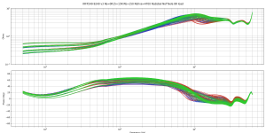
Here is the HF plot for IRFP versus ALFET, both driven from "as low as it would go" impedance, that's 50R from the network analyzer, 20R gate resistor, and ferrite bead.
While the ALFETs definitely have lower capacitance and it shows, the second pole is quite similar for both, which means the extra speed of the ALFETs may not actually be usable, as both would want ULGF below 10MHz. So the verticals are still winning based on lower high order harmonics.
Attachments
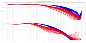
The bipolars are back.
MJL1302/3281, with 20R base resistors and a ferrite bead each, driven by MJE15030-15031 with 75R base resistors, and a 68R resistor between the emitters to set driver idle current.
Supply voltage is stepped so the transistors have from 5V to 25V headroom.
Without a load on the output:

As the datasheet says, transition frequency of bipolars does depend on current. When current is low, fT is low. Three different bias currents are shown, 50mA 100mA 200mA, and the high frequency performance of the output transistors follows the bias current.
Next plot has output load current applied: (-2, -1, -0.5, 0, .5, 1, 2) Amps. All the curves where the devices have enough current to increase their fT are well grouped and show a clean 2-pole lowpass characteristic. The one with zero output current stands out.

Compared with the FETs, it is clear that bipolars have much more phase shift.

The comparison isn't entirely fair because the EF2 with two transistors having similar fT is a 2-pole system, whereas I didn't put drivers on the FETs, which makes them single-pole. But the FETs have more current gain than the EF2 up to a few kHz, and they can be driven by lower current, much higher fT transistors, than good old MJE15030.
FETs win this round again.
BJTs do degrade less at low Vce, though.
MJL1302/3281, with 20R base resistors and a ferrite bead each, driven by MJE15030-15031 with 75R base resistors, and a 68R resistor between the emitters to set driver idle current.
Supply voltage is stepped so the transistors have from 5V to 25V headroom.
Without a load on the output:
As the datasheet says, transition frequency of bipolars does depend on current. When current is low, fT is low. Three different bias currents are shown, 50mA 100mA 200mA, and the high frequency performance of the output transistors follows the bias current.
Next plot has output load current applied: (-2, -1, -0.5, 0, .5, 1, 2) Amps. All the curves where the devices have enough current to increase their fT are well grouped and show a clean 2-pole lowpass characteristic. The one with zero output current stands out.
Compared with the FETs, it is clear that bipolars have much more phase shift.
The comparison isn't entirely fair because the EF2 with two transistors having similar fT is a 2-pole system, whereas I didn't put drivers on the FETs, which makes them single-pole. But the FETs have more current gain than the EF2 up to a few kHz, and they can be driven by lower current, much higher fT transistors, than good old MJE15030.
FETs win this round again.
BJTs do degrade less at low Vce, though.
The comparison isn't entirely fair because the EF2 with two transistors having similar fT is a 2-pole system, whereas I didn't put drivers on the FETs, which makes them single-pole. But the FETs have more current gain than the EF2 up to a few kHz, and they can be driven by lower current, much higher fT transistors, than good old MJE15030.
BJTs do degrade less at low Vce, though.
My favorite is 2SC5171 for driver.
This time I left the supply voltages at +/-25V and stepped the output current. As expected, fT of the output devices follows. Bias is 50mA, and color means higher DC output current.

Removing the 47µF 25V EEUFM capacitor between driver bases: no change.
Increasing drivers idle current from 17mA to 43mA confirms this is about the fT of the power transistors, not the drivers. Although it does raise HF response a little bit.

DarlingtonEF2 configuration:

Pure Darlington configuration:

Back to original EF2, with Thiele network at the output: improves phae margin a bit at 2-3MHz.

MOSFETs win on bandwidth.
Removing the 47µF 25V EEUFM capacitor between driver bases: no change.
Increasing drivers idle current from 17mA to 43mA confirms this is about the fT of the power transistors, not the drivers. Although it does raise HF response a little bit.
DarlingtonEF2 configuration:
Pure Darlington configuration:
Back to original EF2, with Thiele network at the output: improves phae margin a bit at 2-3MHz.
MOSFETs win on bandwidth.
My favorite is 2SC5171 for driver.
Looks nice, but difficult to find! Have you got a source?
I tried 2SA2039/2SC5706 ; they are available, very high fT but low voltage and poor thermals, so these would need to be bootstrapped.
Makes no difference to the behavior of the power devices, but the drivers' pole moves up, with a nice improvement in phase margin.
Attachments
Other drivers:
D44H11/D45H11 with 68R between emitters, pretty much the same as MJE15030-1

IRF610-9610 with 68R between emitters

IRF610-9610 with 68R between emitters

FET drivers do offer better phase margin, that's interesting.
D44H11/D45H11 with 68R between emitters, pretty much the same as MJE15030-1
IRF610-9610 with 68R between emitters
IRF610-9610 with 68R between emitters
FET drivers do offer better phase margin, that's interesting.
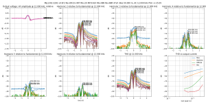
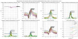
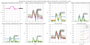
I will now run the automated distortion test on all of these. Since this is bipolar day, the constant will be MJL1302/3281, 0R33 emitter resistors, and 20R base resistors. And the variable will be drivers.
First in line is IRFP9/610 as drivers.
Input capacitance is typical of FETs, ie highly variable with headroom. The two are well matched.

Below is the same plot as before, each trace is a value of output voltage, and the horizontal axis is output current. I removed the illegible text labels and instead simply used Black for zero output voltage.

Bias current varies quite a lot with output voltage. I don't know if this is due to Early effect (or the equivalent for FETs) in the drivers, or Vce-dependent hFe variation in the power devices. I think it's the former.
1) On the bottom left wingspan plot, the black curve is thus the gm wingspan at zero output voltage, and the others over the range of output voltages. Since FET Vgs varies, bias also varies depending on output voltage. This may be a problem if the load is evil enough to make the current switch signs at voltages far from 0V. In this case a two-transistor biasing circuit that keeps the voltage between power transistor bases constant could be a better choice.
2) Likewise, FET current gain depends a bit on Vds. So on the right plots showing current gain, it varies quite a bit depending on output voltage. But one of these lines is perfectly flat, and the different current gains of both FETs compensates exactly the difference in hFe between the power transistors.
3) FETs like headroom, and these want a bootstrap supply.
This offers an interesting possibility: if the FETs are bootstrapped, then their Vds becomes constant, which eliminates problem 1) above. And it is possible to choose a bootstrap supply voltage for each FET that will tweak its gain just right, to make the current gain of the whole stage constant over the whole current range. I think this is the simplest way to achieve this with BJTs. As the HF measurements showed, FETs also offer higher speed and better phase margin than the usual 30MHz fT BJT drivers. Quite interesting.
Now, distortion vs DC output current operating point, output voltage, and amplitude of 12kHz AC output signal. One bias point per plot: 15mA, 50mA, 100mA, 200mA. The FET graphs are here for comparison.
What we're looking for is the amplitude of harmonics going down fast with increasing harmonic order. Each harmonic has its own little plot.
The current holder of the title is IRFP240/9240, which gives identical results for either two pairs at 100mA or one pair at 200mA bias... and it is still winning.
First in line is IRFP9/610 as drivers.
Input capacitance is typical of FETs, ie highly variable with headroom. The two are well matched.
Below is the same plot as before, each trace is a value of output voltage, and the horizontal axis is output current. I removed the illegible text labels and instead simply used Black for zero output voltage.
Bias current varies quite a lot with output voltage. I don't know if this is due to Early effect (or the equivalent for FETs) in the drivers, or Vce-dependent hFe variation in the power devices. I think it's the former.
1) On the bottom left wingspan plot, the black curve is thus the gm wingspan at zero output voltage, and the others over the range of output voltages. Since FET Vgs varies, bias also varies depending on output voltage. This may be a problem if the load is evil enough to make the current switch signs at voltages far from 0V. In this case a two-transistor biasing circuit that keeps the voltage between power transistor bases constant could be a better choice.
2) Likewise, FET current gain depends a bit on Vds. So on the right plots showing current gain, it varies quite a bit depending on output voltage. But one of these lines is perfectly flat, and the different current gains of both FETs compensates exactly the difference in hFe between the power transistors.
3) FETs like headroom, and these want a bootstrap supply.
This offers an interesting possibility: if the FETs are bootstrapped, then their Vds becomes constant, which eliminates problem 1) above. And it is possible to choose a bootstrap supply voltage for each FET that will tweak its gain just right, to make the current gain of the whole stage constant over the whole current range. I think this is the simplest way to achieve this with BJTs. As the HF measurements showed, FETs also offer higher speed and better phase margin than the usual 30MHz fT BJT drivers. Quite interesting.
Now, distortion vs DC output current operating point, output voltage, and amplitude of 12kHz AC output signal. One bias point per plot: 15mA, 50mA, 100mA, 200mA. The FET graphs are here for comparison.
What we're looking for is the amplitude of harmonics going down fast with increasing harmonic order. Each harmonic has its own little plot.
The current holder of the title is IRFP240/9240, which gives identical results for either two pairs at 100mA or one pair at 200mA bias... and it is still winning.
Attachments
-
 thd-MJL1302-3281 v4 EF2 Re=0R33+4R7 Rb=20 IRF9-610 Rb=488 Re=68R 47uF-B=50.0m,HA=5.0m,LA=2500.0m.png345.3 KB · Views: 335
 -
 thd-MJL1302-3281 v4 EF2 Re=0R33+4R7 Rb=20 IRF9-610 Rb=488 Re=68R 47uF-B=15.0m,HA=5.0m,LA=2500.0m.png324 KB · Views: 325
 -
 thd-MJL1302-3281 v4 EF2 Re=0R33+4R7 Rb=20 IRF9-610 Rb=488 Re=68R 47uF-B=200.0m,HA=5.0m,LA=2500.0.png333 KB · Views: 326
 -
 thd-MJL1302-3281 v4 EF2 Re=0R33+4R7 Rb=20 IRF9-610 Rb=488 Re=68R 47uF-B=100.0m,HA=5.0m,LA=2500.0.png336.5 KB · Views: 315
Last edited:
I think a 20R base resistor is far too high. 4R7 and 2R2 are more common if they are used at all. Also, can you try a diamond buffer please?
-Chris
-Chris
Looks nice, but difficult to find! Have you got a source?
I bought from local store. Some of my friends sale it at local online store. I do not know where their source.
I think a 20R base resistor is far too high. 4R7 and 2R2 are more common if they are used at all. Also, can you try a diamond buffer please?
Yeah, I'm going to lower the base resistor value. Earlier I tried 0R (just the ferrite bead) and it oscillated. I will try 4R7.
Diamond buffer drivers would require 2 current sources providing the maximum base current for the power devices at all times, which would significantly increase idle dissipation... Going with hFe of 100 and max output current of 10A, that would be two 100mA current sources... Did you mean diamond buffer predrivers?
I bought from local store. Some of my friends sale it at local online store. I do not know where their source.
Can you share the url of the online store?
Can you share the url of the online store?
https://www.tokopedia.com/kusalaelectro/a1930-c5171-2sa1930-2sc5171
Hi Peufeu,
This is great work! I really appreciate you (and others) who do some real research and puts it out here for everyone to read and participate in the discussion.
That said, I agree with anatech that 20R base resistor on the BJT output transistors is too high. It will modulate the idle current of the output stage with the signal. It will also make the output stage more dependent on beta matching between P and N transistors. Cordell mentions this in his book.
Like anatech said, you wouldn't build a real output stage with base resistors that large so it causes us to question if your results are valid for a normal output stage where those resistors are removed.
The AD8421 can be configured for a large gain (at the cost of BW) so why not use base resistors <1ohm and increase the gain of AD8421? Any potential decrease in SNR on the measured base current might not matter much?
- Home
- Amplifiers
- Solid State
- Power amp OUTPUT STAGE measurements shootout