No no, the goal is to compare output stages, which involves this question:
"In the final distortion result (complete amp, closed loop) how much distortion is added to the output if:
1) the output stage adds X volts distortion
2) the output stage pulls Y nonlinear current"
Spice answers:

V7 is set to 1V AC (in blue, representing distortion as a voltage added by the output stage to the VAS output node). Since the amp uses second order compensation, at 1kHz it is reduced by a huge factor of 220k. To get the same output distortion by injecting a current into the VAS node, current source I3 would need to be set to AC 50µA (red). So to compare the influence of voltage and input current nonlinearities in this output stage, a source impedance of 20k should be used (at 1kHz). That corresponds more or less to the open loop output impedance of this VAS.
"In the final distortion result (complete amp, closed loop) how much distortion is added to the output if:
1) the output stage adds X volts distortion
2) the output stage pulls Y nonlinear current"
Spice answers:
V7 is set to 1V AC (in blue, representing distortion as a voltage added by the output stage to the VAS output node). Since the amp uses second order compensation, at 1kHz it is reduced by a huge factor of 220k. To get the same output distortion by injecting a current into the VAS node, current source I3 would need to be set to AC 50µA (red). So to compare the influence of voltage and input current nonlinearities in this output stage, a source impedance of 20k should be used (at 1kHz). That corresponds more or less to the open loop output impedance of this VAS.
Try to add some kind of buffer (simply EF) behind VAS and inject disturbig current in output node of this buffer. Differences will be marginal. IMO your simulation show contamination from bad PSSR, imperfection of active load for VAS.
Last edited:
Hi peufeu,
This is what will be most helpful. The lower the distortion contributed by the output stage, the less NFB has to compensate for and you will end up with the cleaner amplifier - all other things held equal.
-Chris
Exactly!!!!the goal is to compare output stages
This is what will be most helpful. The lower the distortion contributed by the output stage, the less NFB has to compensate for and you will end up with the cleaner amplifier - all other things held equal.
-Chris
Exactly.
Next phase is going nicely. I've added an output relay to disconnect the load. So when driving the input, it will measure input current without load, which is basically input capacitance. Then the relay closes, and it is measured again, this time with output current. Then it does the previous test, driving the output. Vce for both transistors is stepped, so tomorrow I should have a graph of what happens to the MOSFETs when the output gets near the rails.
Theory (and the gate current on the scope) says capacitance increases quite a lot, things get nasty, and the annoying fact is that the MOSFET that has low Vds is of course the one that is on (assuming that when the output voltage is close to the rail, output current should be high enough to turn off the other FET). So we'll see what happens to fT in this situation. This matters as the amp should not oscillate near clipping, which means it should be compensated for the worst case behavior of the FETs.
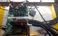
This is the "new and improved" setup:

Instead of using the two drive amps to drive the bases/gates, I'm using one drive amp, and a Vbe multiplier (also programmable) to set the bias. The relay in the output disconnects the load.
In a real amplifier, the input voltage would swing all the way to clipping, but in this one, the instrumentation amplifiers don't have that much input common mode range. So, instead:
- Output voltage is still 0V DC
- Input is driven with low level AC
- Power supply voltages are stepped (both bench PSUs are programmable).
From the point of view of the output stage, this is just like being in a real amplifier. For example, if the virtual amplifier would have +/-12V power supplies, to test at a a virtual output voltage of +5V DC, I'd simply set the positive power supply to +7V, the OPS output to 0V, and negative power supply to -19V.
Driving the input without load, input current is basically input capacitance of this OPS. So... here it is:

This confirms what is already known: with MOSFETs, input capacitance goes YOLO when the gate voltage goes above the drain (or below for PMOS). For these specific FETs, that happens when the output reaches about 5V from the rails.
When using a higher power supply voltage for the virtual amp, one of the bench PSUs reaches its maximum voltage too soon, and that inserts a suspicious looking dimple in the capacitance, but it's just a measurement artifact.

Instead of using the two drive amps to drive the bases/gates, I'm using one drive amp, and a Vbe multiplier (also programmable) to set the bias. The relay in the output disconnects the load.
In a real amplifier, the input voltage would swing all the way to clipping, but in this one, the instrumentation amplifiers don't have that much input common mode range. So, instead:
- Output voltage is still 0V DC
- Input is driven with low level AC
- Power supply voltages are stepped (both bench PSUs are programmable).
From the point of view of the output stage, this is just like being in a real amplifier. For example, if the virtual amplifier would have +/-12V power supplies, to test at a a virtual output voltage of +5V DC, I'd simply set the positive power supply to +7V, the OPS output to 0V, and negative power supply to -19V.
Driving the input without load, input current is basically input capacitance of this OPS. So... here it is:
This confirms what is already known: with MOSFETs, input capacitance goes YOLO when the gate voltage goes above the drain (or below for PMOS). For these specific FETs, that happens when the output reaches about 5V from the rails.
When using a higher power supply voltage for the virtual amp, one of the bench PSUs reaches its maximum voltage too soon, and that inserts a suspicious looking dimple in the capacitance, but it's just a measurement artifact.
It works.
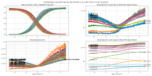
The output voltage of this virtual amplifier moves by moving the power supplies. The little labels on the plots say "+xxV/-xxV" which are the supply voltages. So, if it says "+25/-5" it means the NMOS has 25V headroom and the PMOS has 5V.
The output current is swept over the full +/-1.5A range no matter what the output voltage is. It's a bit unrealistic to output a negative current while it is stuck against the positive rail, but hey, it would have been much more complicated not to do it, and it's free.

gm is pretty much the same whether it is measured by driving the input or the output. That's expected, because gm is d(Iout)/d(V(in,out)) so it depends on the difference between input voltage and outptu voltage, which is the same in both cases. It also does not change much with output voltage.
Current gain is another story. With the output being driven, as in the previous tests, it is very high, and changes very little with output voltage, until clipping where it drops. This is because the input voltage isn't moving, so both Vds are quite constant, and Cds capacitances are out of the picture. It's like having a cascode. So the good news is, it says what a cascoded output stage would do.
However when driving the input, as in a real amplifier, Cgd really matters. It is this capacitance that varies most with output voltage (and thus Vds headroom). Since it sucks out a significant part of the gate current, current gain is reduced substantially.
As long as the FET gates don't go over the rails, which means the output is more than 5V away from the rails, it's quite fine, current gain is pretty smooth and varies around 1-2k. But near the rails, it really drops.
I've made another plot with the same data, except X axis is the output voltage.

These are MOSFETs, so caveat: current gain is inversely proportional to frequency. These plots are at 12kHz, so at 120Hz, current gain would be 100x what the plot shows.
The output voltage of this virtual amplifier moves by moving the power supplies. The little labels on the plots say "+xxV/-xxV" which are the supply voltages. So, if it says "+25/-5" it means the NMOS has 25V headroom and the PMOS has 5V.
The output current is swept over the full +/-1.5A range no matter what the output voltage is. It's a bit unrealistic to output a negative current while it is stuck against the positive rail, but hey, it would have been much more complicated not to do it, and it's free.
gm is pretty much the same whether it is measured by driving the input or the output. That's expected, because gm is d(Iout)/d(V(in,out)) so it depends on the difference between input voltage and outptu voltage, which is the same in both cases. It also does not change much with output voltage.
Current gain is another story. With the output being driven, as in the previous tests, it is very high, and changes very little with output voltage, until clipping where it drops. This is because the input voltage isn't moving, so both Vds are quite constant, and Cds capacitances are out of the picture. It's like having a cascode. So the good news is, it says what a cascoded output stage would do.
However when driving the input, as in a real amplifier, Cgd really matters. It is this capacitance that varies most with output voltage (and thus Vds headroom). Since it sucks out a significant part of the gate current, current gain is reduced substantially.
As long as the FET gates don't go over the rails, which means the output is more than 5V away from the rails, it's quite fine, current gain is pretty smooth and varies around 1-2k. But near the rails, it really drops.
I've made another plot with the same data, except X axis is the output voltage.
These are MOSFETs, so caveat: current gain is inversely proportional to frequency. These plots are at 12kHz, so at 120Hz, current gain would be 100x what the plot shows.
As seen before, hFe mismatch between the top and bottom drivers was a problem with BJTs, because the base current of each transistor tends to go through its corresponding driver only. So driver hFe mismatch causes a large jump in total current gain at crossover.
This is not the case with these FETs, because the gate current is the same whether they're on or off. Gate current simply charges the FET capacitances according to voltage variations, but unlike BJTs it has no relation to emitter current. So driver hFe mismatch does nothing to the FET crossover. It does tilt the picture a bit when we get near the rails, because the FET that is being squeezed does draw more current as its capacitance increases, but this is a large signal effect and thus not really a problem.
This is another significant difference between BJTs and FETs, it seems.
In the following plot I've simulated a driver having double the hFe of the other.
Attachments

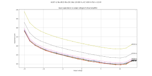
There was a mistake in the previous curves: the voltages displayed in text were the input voltages, not the output voltages. So, with the IRFP FETs, capacitance increases dramatically when Vgs becomes higher than Vds. That does correspond to an input voltage about 5V from the rail, but the output voltage will be further away from the rail of course, due to output current.
I've fixed that bug, so now it displays the real Vds of the FETs, these are the numbers on the bottom right graph. And the "output voltage" on the X axis of the second graph is also the real output voltage with the full test current of 2.5A.


So the required headroom for clean operation is about 7 volts.
All gm curves are still on top of each other, which means it doesn't change much with headroom and gm stays strong even at high current, which is nice.
What really changes is how much drive current it takes.
Now accounting for Cds, when they have enough headroom, the transition frequency of these FETs is no longer that awesome, about 20-30 MHz. Less glorious than anticipated, but still on par with the fast bipolars, and even a few volts from the rail, the FETs still have better current gain and smoother low order distortion. So, not that bad.
Lateral FETs show a completely different picture.

As shown before, both gm and current gain are way uglier.
Gm drops much more at high current and low headroom with the laterals than with the IRFP9/240. The bottom two curves are at 5V Vds for the corresponding FETs, and they're struggling.
However, their capacitance is lower, and it increases less dramatically at low Vds, which means they're faster, fT is higher, and it stays higher closer to the rail.

What is not really shown on the graphs is that at max current the Vds is close to 5V and that's it. You can drive the gate harder, it won't squeeze more juice. So while it looks like they'd need less headroom than the vertical FETs, that's not actually the case. The verticals can go closer to the rail and they get very slow in doing so ; the laterals can't so they stay fast.
I've fixed that bug, so now it displays the real Vds of the FETs, these are the numbers on the bottom right graph. And the "output voltage" on the X axis of the second graph is also the real output voltage with the full test current of 2.5A.
So the required headroom for clean operation is about 7 volts.
All gm curves are still on top of each other, which means it doesn't change much with headroom and gm stays strong even at high current, which is nice.
What really changes is how much drive current it takes.
Now accounting for Cds, when they have enough headroom, the transition frequency of these FETs is no longer that awesome, about 20-30 MHz. Less glorious than anticipated, but still on par with the fast bipolars, and even a few volts from the rail, the FETs still have better current gain and smoother low order distortion. So, not that bad.
Lateral FETs show a completely different picture.
As shown before, both gm and current gain are way uglier.
Gm drops much more at high current and low headroom with the laterals than with the IRFP9/240. The bottom two curves are at 5V Vds for the corresponding FETs, and they're struggling.
However, their capacitance is lower, and it increases less dramatically at low Vds, which means they're faster, fT is higher, and it stays higher closer to the rail.
What is not really shown on the graphs is that at max current the Vds is close to 5V and that's it. You can drive the gate harder, it won't squeeze more juice. So while it looks like they'd need less headroom than the vertical FETs, that's not actually the case. The verticals can go closer to the rail and they get very slow in doing so ; the laterals can't so they stay fast.
Two extra plots:
Input capacitance plot for the laterals, that I forgot to add earlier. It is much lower than the vertical FETs.
IRFP9/240 at 240mA bias. With the laterals, more bias doesn't make the crossover smoother. With the verticals, it does.
Input capacitance plot for the laterals, that I forgot to add earlier. It is much lower than the vertical FETs.
IRFP9/240 at 240mA bias. With the laterals, more bias doesn't make the crossover smoother. With the verticals, it does.
Attachments
Is anyone still reading? lol
One funny thing with MOSFETs is, current gain is not really current gain.
Since most of the gate current goes to the drain capacitance, input current depends a lot more on output voltage dv/dt, than on output current (and therefore load impedance).
Whether the load is 4 ohms, 8 ohms or whatever, a little bit more or a little bit less of the current will have to go to Cgs to set Vgs to actually output the required current. But most of the gate current will still go to Cds.
The result is the apparent current gain depends on load impedance, but in a good way: when impedance is divided by 2, input current increases only a little bit, which means apparent current gain increases.
Example with IRFP9/240 at 50mA bias (a bit stingy I know)...
8R load, 12 kHz, 0A output current: apparent current gain 2500
4R load, 12 kHz, 0A output current: apparent current gain 3500
...and at the same output power
8R load, 12 kHz, +1A output current: apparent current gain 4000
4R load, 12 kHz, +2A output current: apparent current gain 7500
So the driving stages are pretty well isolated from impedance dips in the load.
Now there is one annoying thing with these IRFP MOSFETs: they need 150-200 mA bias current to have smooth flat gm and current gain. So that brings several questions:
1) Does it matter?
2) How that works with multiple parallel devices
Adding more devices in parallel increases input capacitance. So with MOSFETs it will reduce total current gain in proportion.
If total bias current stays constant, then adding devices means each one runs at a lower bias, so we get higher total current capability, but uglier gm and current gain (on top of higher capacitance). However, if each device gets an equal share of the output current, then their gm and current gain curves will be "stretched" (ie, widened) so the derivatives of that transferfunction will be divided by the number of transistors, and since distortion depends on that, it will be reduced.
So it is not obvious whether one pair of devices at 200mA will beat two pairs at 100mA each...
@peufeu Is your research focused only on Class AB? Can we assume all these non-linearities are gone once we employ Class A? Do you consider investigating differences between various implementations of Class A by your method?

Bootstrapped cascode removes >90% of Cgd and >90% of Cgs. But it forces you to spend additional money on additional VAs for your power transformer. Same I, bigger V, thus bigger I*V product. More money for higher voltage rail caps too. Oh and twice as many output transistors ... but less dissipation per device so greater reliability.
Congratulations
😀
Bootstrapped cascode
I think I'm going to try it.
@peufeu Is your research focused only on Class AB
I would say it's about finding the best compromise, ie distortion close to class A, dissipation close to class AB, have your cake and eat it 😀
But for that, we need a distortion metric that actually works. I said I'd use the Gedlee metric, because it has been tested on people and correlates with listening results. The math is very simple, it's the weighted RMS sum of the second derivative of the transfer function.
I don't want to take derivatives of noisy signals. Additionally in the case of the LATFETs it would be headache inducing to compute it with enough accuracy because of the two sharp dips. So instead, I just make the DUT do the math all by itself: by driving the input with a low amplitude high frequency signal and sweeping the output current, the amplitude of this HF signal in the output is then proportional to the first derivative of the input->output transfer function. Distortion harmonics on this small signal correspond to the other derivatives.
So basically, throwing away all constants because yolo, we're doing comparisons:
Gedlee metric is similar in spirit to taking the THD on a low amplitude signal, while sweeping the DC output current... and looking either at the max value of this THD, or a weighted average centered on low output currents which is where the amp spends most of its time.
How the test is done:
1) The DUT is driven from its input (like in a real amp) with a low amplitude, 12kHz sine of varying amplitude. DC input voltage is zero.
2) The output is connected via a 8R load to the output of the Modulus-86 which plays a low frequency sine wave, which pushes and pulls current in and out of the output stage. This sets the "DC" operating point of the DUT. It is equivalent to driving the input with a voltage that would make it output the same current into a resistor, but it is much easier to measure this way.
3) Output voltage is measured, and harmonics of the 12kHz tone are extracted by simple detection (no FFT) so they are not averaged over the whole period of the LF signal that does the current sweep. Instead that gives the "instantanous" amplitude of each harmonic, averaged over one 12kHz period, which is short enough to consider the LF current injected into the output as constant, ie, the same as DC operating point.
TL/DR: it gives the distortion harmonics of the small signal at each value of output current.
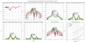
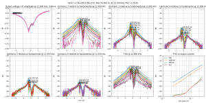
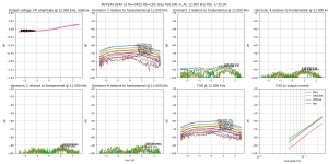
Results for vertical FETs at three bias currents below.
Labels on plots are the small signal amplitudes. So for example on the "harmonic 2" plot it shows the H2 of a 12kHz signal corresponding to an AC output current value that's written on the graph, with DC output current on the X axis.
The same measurement could be done with standard gear by connecting an adjustable DC current source to the output of the amp to draw a DC current from the output, and then doing an AC-coupled THD measurement at various values of DC current. However with this method, the bias would probably drift, it would only heat one transistor, etc. I'm using a 40Hz sine instead of a current source, because that behaves more like music, it heats both transistors equally, the bias does not drift, and it is quick.
Anyway, here's the IRFP9/240 compared to the ALFETs, at bias 50mA,100mA,200mA. All the plots use the same scales, so you can quickly compare by switching between the pictures.
Attachments
-
 thd-ALFET v2 Re=0R15 Rb=150-B=200.0m,HA=5.0m,LA=2500.0m-F=12k.png402.3 KB · Views: 135
 -
 thd-ALFET v2 Re=0R15 Rb=150-B=100.0m,HA=5.0m,LA=2500.0m-F=12k.png440 KB · Views: 343
 -
 thd-ALFET v2 Re=0R15 Rb=150-B=50.0m,HA=5.0m,LA=2500.0m-F=12k.png456.6 KB · Views: 338
 -
 thd-IRFP240-9240 v2 Re=0R15 Rb=150-B=200.0m,HA=5.0m,LA=2500.0m-F=12k.png338.2 KB · Views: 334
 -
 thd-IRFP240-9240 v2 Re=0R15 Rb=150-B=100.0m,HA=5.0m,LA=2500.0m-F=12k.png397.7 KB · Views: 330
 -
 thd-IRFP240-9240 v2 Re=0R15 Rb=150-B=50.0m,HA=5.0m,LA=2500.0m-F=12k.png432.5 KB · Views: 337
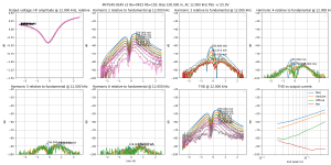
So what do the plots say?
THD on this AC small-signal depends a lot on the "DC" current.
There is a minimum around zero output current, that corresponds to the point where Gm has a flat bottom. But it is not exactly at zero output current. It depends on device matching, how the slopes of both devices meet, etc.
A standard THD vs level with the output voltage (and current) centered on zero only samples one point on this characteristic curve. It will probably give different results depending on where the minimum is relative to zero... So I guess "device matching is important for THD" can be translated as "it moves the minimum around, and when you get lucky it puts the minimum just where you measure so it looks better!"
Whereas by measuring it over the entire range of current, it gives a much clearer picture, and I feel it gives more useful info about how it will behave with music.
The bottom right plot uses a different X axis, which is the peak amplitude of the 12kHz signal whose distortion is measured. So it is a simple THD vs level plot. Its curves are:
"Max" and "Min" are the maximum THD over the whole DC current range.
"Official" is the THD minimum around zero output current, that is found by the dude who turns the bias pot while looking at the THD meter. That one goes in the brochure.
"GedLike" is the average THD on the 12k sine with DC output current of -1..+1 DC amps, RMS-cosine-weighted, like in the Gedlee metric paper.
Soooo....
The IRFP9/240 have an interesting characteristic: by increasing the bias, gm gets smoother, and the higher harmonics disappear.
Whereas the LATFETs do not have this characteristic: increasing the bias pushes the points with the maximum higher harmonics to higher output current values, and reduces the level a bit, but it's just not that good.
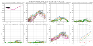
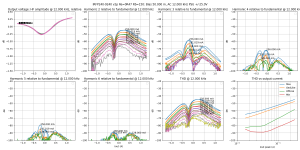
Another fun thing is to compare graph #2 and graph #3, IRFPs at 100mA and 200mA.
At 200mA the distortion minimum near zero output current disappears, because the hole in the middle of the gm curve gets filled and the bottom is not flat, it has a bit of a slope due to device mismatch.
So the guy who tweaks the bias pot while looking at the THD meter concludes "above 100mA bias, distortion goes up! There must be... an optimal bias point!"
In fact, at 200mA, distortion and especially higher harmonics are massively reduced everywhere at all DC current values... except in the distortion minimum around zero, which just disappeared when increasing the bias, and that was just the point that the usual measurements look at, while ignoring the rest.
With the huge heat sink, I can crank the bias to 400mA. It stabilized at 500mA during the test.
Every harmonic is wiped clean except the 2nd. Near zero output current, it is higher than at lower bias, which gives the illusion that increasing the bias doesn't help. But that's an illusion...
I really like this feature of vertical FETs. A good circuit should be able to fix or work around their other defects.
However there is no workaround for the higher order distortion products of laterals, which means they lose this round.
Attachments
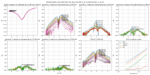
So who wins? One pair of IRFP's biased at 100mA? Two pairs biased at 50mA?
Two pairs of FETs have double the input capacitance, so they need twice the drive current. Their Vgs swings will be halved but that does not matter, as most of the gate current goes into the drain capacitance.
That's not really a problem, and a price worth paying for 2x better thermals. (Note this would be different for BJTs, as the part of base current that is Iout/hFe would be shared between both devices, only the capacitive part would double).
There's only space for one pair in the setup, so I emulated two pairs by doubling the load resistor, so all currents are halved, while all voltages stay the same.
The difference between one pair of FETs at 100mA bias, and two pairs at 50mA each is... not spectacular. Two pairs has slightly lower distortion across output currents, that's all.
It's the same story at 2x100mA vs 1x200mA.
This is excellent news, but there is a fine print.
Attachments

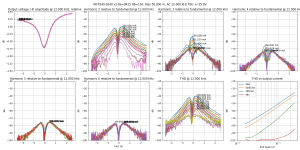
The fine print is:
1) if the derivative of f(x) is f'(x) then
the derivative of f( 1/2 x) is 1/2 f'( 1/2 x)
the second derivative is 1/4 f"( 1/2 x)
TL/DR: if you stretch the X "current" axis by a factor of 2 by halving the current per device, the n'th derivative of the transfer function is divided by 2^n which does wonders to high order harmonics. This will work for all devices, so more devices in parallel at the same bias per device should always work better no matter the device, it's just math but it burns more electricity of course.
2) However these FETs have a different property: more devices in parallel works just as well with the same total bias, ie less bias per device which is a different thing. The above math no longer applies since the transfer function of one pair at one bias is not the same with half bias. But these FETs have a nice smooth gm curve which is a mix of exponential in subthreshold and square law above that, which means gm "scales" just right to make the transfer function of two pairs at half bias almost identical to one pair at full bias.
If this gm characteristic is screwed by using a high source resistor, it no longer works.
The previous test was with 0R15 source resistors in all cases.
If, while doubling the devices and halving the bias per device, I replace the 0R15 resistor with a 0R47 resistor, then it is worse. Higher order harmonics go up significantly.
It looks like this topic is turning into "scientific proof Lord Pass knows what he's doing" 😀
Attachments

Last edited:
- Home
- Amplifiers
- Solid State
- Power amp OUTPUT STAGE measurements shootout