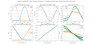
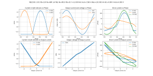
I noticed the slope of the current gain of the FQP FETs was opposite to the one of the MJL1302/3281 BJTs.
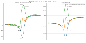
So I wired the FQP3N30/FQP3P20 as drivers, idling at about 20mA. Then, MJL1302/3281, with 0R33 emitter resistors.

This gives an output stage with current gain of 100 000 at 48kHz (shown on graph) and due to the FETs, it is inversely proportional to frequency, which means 240 000 at 20kHz.
Gm is identical to the BJT stage, but if this thing was current driven, then an interesting property is the current gain doesn't vary that much over the measured +/-1A output range.
Combine with bootstrapped drivers to cancel drain capacitance variation, and I think this would be an interesting candidate.


I will compare with a darlington using BJTs as drivers.
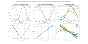
So I wired the FQP3N30/FQP3P20 as drivers, idling at about 20mA. Then, MJL1302/3281, with 0R33 emitter resistors.
This gives an output stage with current gain of 100 000 at 48kHz (shown on graph) and due to the FETs, it is inversely proportional to frequency, which means 240 000 at 20kHz.
Gm is identical to the BJT stage, but if this thing was current driven, then an interesting property is the current gain doesn't vary that much over the measured +/-1A output range.
Combine with bootstrapped drivers to cancel drain capacitance variation, and I think this would be an interesting candidate.
I will compare with a darlington using BJTs as drivers.

J. Curl uses MOSFET drivers and BJT output transistors (Sanken 60 MHz) in his Parasound power amps.
Could you do a Cascoded Mosfet/BJT combination at some point? Would be interesting to see how that reacts.
J. Curl uses MOSFET drivers and BJT output transistors (Sanken 60 MHz) in his Parasound power amps.
Yes, it looks like a good combo, I guess he knows what he's doing 😀
Could you do a Cascoded Mosfet/BJT combination at some point? Would be interesting to see how that reacts.
Right now I'm driving the output so it is pretty much like having a cascode. It's a quick test so I started with that to weed out the combos that have a bad crossover. Also I'm using pretty low Vce (15V) to avoid too much heating and the bias changing during the test.
Next I'm going to drive the input while stepping the DC to measure response at various Vds/Vce voltages, to cover the whole range of parameters an output stage goes through with real signal...
Last edited:
The Revox B242 also used Mosfets as drivers for BJT outputs. That isolates the Vas from output load variations to some degree.
Alright!
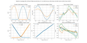
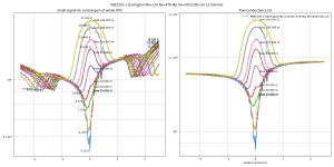
Next is a face-off between darlington and the classic Emitter Follower 2 (EF2).

They look quite close, since the only difference is one resistor. On the EF2 the resistor between emitters is 68 ohms.
(the previous experiment with FQP MOSFETs driving the bipolars was an EF2 topology with MOSFET drivers).
The darlington topology with bipolar power devices gives a gm plot typical of bipolars. The current gain is high, and it looks exactly like a scaled up version of the gm plot. This is logical, as current through the drivers is heavily dependent on Vbe of the pass devices, because driver emitter resistors are across these Vbe junctions.
These graphs show lots of different bias currents at once.

At the optimum bias of about 60mA (for 0R33 emitter resistors) current gain varies about 40%, and averages at 10k.
Of note is a heavy loss of current gain at higher frequency and high current. I don't like this feature.

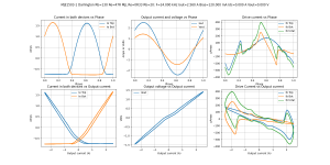
Comparing with EF2 using the exact same transistors: gm is almost the same, but...
With darlingtons, the bias current in the emitter resistors is the total bias current, driver plus power device. With EF2, it is only the bias current through the power devices. So, the EF2 burns 20 mA more than what the legend says, which means when comparing curves, the EF2 at 40mA should be compared to the Darlington at 60mA, if we're scoring on watts burned.
Anyway. 12kHz and 48kHz:


While the gm's are similar, current gain is completely different!
When only one half conducts, current gain of the EF2 output stage is the product of the hFe's of the corresponding driver and power transistor. Same for the other half. And in the middle, when they all conduct, it's an average between the two.
So it works in three modes, visible as three plateaus in the left plot (current gain). When bias is high, the middle plateau with both devices conducting is quite wide. But when bias is low, it is tiny, and current gain jumps abruptly at crossover between the "product of Top transistors hFe" and "product of Bottom transistors hFe" values.
And the difference is large, more than x2, with 15k gain on one side and 37k gain on the other.
How is this possible, when the power devices have a much smaller difference in hFe? I repost the plots from MJL1302/3281 alone, without drivers. Unfortunately it stops at 500mA instead of 1A, but it shows the current gain smoothly transitioning from 100 to 125:

This is far from the x2 value with the drivers:

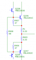
The reason is quite simple when one looks on the schematic:
The emitter output impedance of each driver forms a current divider with the 68R resistor between the drivers, and the driver has much lower impedance than the resistor. At 20mA the driver emitter should be in the 1 ohm range, versus a 68 ohm resistor.
Therefore, almost all the base current for the top transistor goes through the top driver ; same thing for the bottom transistors.
While the hFe of these power transistors are quite close, the drivers have wildly different hFe. And... that explains it.
I attempt a fix, by inserting a 470µF Panasonic FR capacitor between the driver emitters. It has an ESR of about 80-100 mOhms.

The variations in current gain of this output stage are back to 40% instead of x2, much closer than the hFe differences between power devices.
Therefore, the usual speed-up capacitor isn't just there to speed up the turn off of the power transistors. It should also help compensate the difference in hFe between the drivers, at least at high frequency.
Keeping the current gain constant over output current should be beneficial, so there's probably a topology to be invented for this. I believe the circuit between the driver emitters in the Threshold schematic posted by Mark earlier could be there for a similar reason, by acting as a low impedance shunt regulator between the power device bases, it would ensure an equal amount of the base current of each would go through each driver. This is much better than a capacitor, because it works at all frequencies.
One could also mix and match devices, like use a top driver with lower hFe to compensate for the top power device having higher hFe. This is what I did by using FQP's to drive the bipolars. I doubt this kind of cancellation would be applicable in practice without hand sorting/matching devices though.
Another way would be to use a diamond buffer topology, by turning the drivers upside down, the NPN which usually has higher gain, drives a PNP device of lower gain, and vice versa.
Next is a face-off between darlington and the classic Emitter Follower 2 (EF2).
They look quite close, since the only difference is one resistor. On the EF2 the resistor between emitters is 68 ohms.
(the previous experiment with FQP MOSFETs driving the bipolars was an EF2 topology with MOSFET drivers).
The darlington topology with bipolar power devices gives a gm plot typical of bipolars. The current gain is high, and it looks exactly like a scaled up version of the gm plot. This is logical, as current through the drivers is heavily dependent on Vbe of the pass devices, because driver emitter resistors are across these Vbe junctions.
These graphs show lots of different bias currents at once.
At the optimum bias of about 60mA (for 0R33 emitter resistors) current gain varies about 40%, and averages at 10k.
Of note is a heavy loss of current gain at higher frequency and high current. I don't like this feature.
Comparing with EF2 using the exact same transistors: gm is almost the same, but...
With darlingtons, the bias current in the emitter resistors is the total bias current, driver plus power device. With EF2, it is only the bias current through the power devices. So, the EF2 burns 20 mA more than what the legend says, which means when comparing curves, the EF2 at 40mA should be compared to the Darlington at 60mA, if we're scoring on watts burned.
Anyway. 12kHz and 48kHz:
While the gm's are similar, current gain is completely different!
When only one half conducts, current gain of the EF2 output stage is the product of the hFe's of the corresponding driver and power transistor. Same for the other half. And in the middle, when they all conduct, it's an average between the two.
So it works in three modes, visible as three plateaus in the left plot (current gain). When bias is high, the middle plateau with both devices conducting is quite wide. But when bias is low, it is tiny, and current gain jumps abruptly at crossover between the "product of Top transistors hFe" and "product of Bottom transistors hFe" values.
And the difference is large, more than x2, with 15k gain on one side and 37k gain on the other.
How is this possible, when the power devices have a much smaller difference in hFe? I repost the plots from MJL1302/3281 alone, without drivers. Unfortunately it stops at 500mA instead of 1A, but it shows the current gain smoothly transitioning from 100 to 125:
This is far from the x2 value with the drivers:
The reason is quite simple when one looks on the schematic:
The emitter output impedance of each driver forms a current divider with the 68R resistor between the drivers, and the driver has much lower impedance than the resistor. At 20mA the driver emitter should be in the 1 ohm range, versus a 68 ohm resistor.
Therefore, almost all the base current for the top transistor goes through the top driver ; same thing for the bottom transistors.
While the hFe of these power transistors are quite close, the drivers have wildly different hFe. And... that explains it.
I attempt a fix, by inserting a 470µF Panasonic FR capacitor between the driver emitters. It has an ESR of about 80-100 mOhms.
The variations in current gain of this output stage are back to 40% instead of x2, much closer than the hFe differences between power devices.
Therefore, the usual speed-up capacitor isn't just there to speed up the turn off of the power transistors. It should also help compensate the difference in hFe between the drivers, at least at high frequency.
Keeping the current gain constant over output current should be beneficial, so there's probably a topology to be invented for this. I believe the circuit between the driver emitters in the Threshold schematic posted by Mark earlier could be there for a similar reason, by acting as a low impedance shunt regulator between the power device bases, it would ensure an equal amount of the base current of each would go through each driver. This is much better than a capacitor, because it works at all frequencies.
One could also mix and match devices, like use a top driver with lower hFe to compensate for the top power device having higher hFe. This is what I did by using FQP's to drive the bipolars. I doubt this kind of cancellation would be applicable in practice without hand sorting/matching devices though.
Another way would be to use a diamond buffer topology, by turning the drivers upside down, the NPN which usually has higher gain, drives a PNP device of lower gain, and vice versa.
Last edited:
I don't understand everything, but I find it very interesting! I hope you can make a summary for dummies later 🙂 Keep up the good work!
...
One could also mix and match devices, like use a top driver with lower hFe to compensate for the top power device having higher hFe. This is what I did by using FQP's to drive the bipolars. I doubt this kind of cancellation would be applicable in practice without hand sorting/matching devices though.
Another way would be to use a diamond buffer topology, by turning the drivers upside down, the NPN which usually has higher gain, drives a PNP device of lower gain, and vice versa.
Would an EF3 topology be another improvement for this issue? Either in the (simple) variant of the driver emitter R connected to the opposite rail, or in the (more complex) variant of a current source instead or a resistor?
I'm not sure...
Here's the issue. The base current of the top power transistor goes through the top driver, and the base current of the bottom power transistor goes through the bottom driver. So each base current gets a different driver hFe. Even if the power transistors have a good hFe match, if the drivers don't, then there will be a sharp change in current gain at crossover.
Predrivers in an EF3 stage would reduce the drive current needed fro mprevious stage (by adding another hFe), but they wouldn't do anything against this distortion mechanism. I've come up with several ideas, but that'll have to wait.
I have to finish the darlington first.
Alright... the darlington, with 47R resistor, you know which one, there's only one in a darlington.
It turned out the test current was too low. It wasn't high enough to hit the point where the darlington drivers turn off, which is where they lose it.
I have procured chunkier power resistors from the junk bin to solve this problem, and the test current has been increased to a few amps. The heat sinks are still too small, so the bias current indicated on the graphs is bogus : during the test it is about 50% more.
I think the base current graphs speak for themselves, about why having drivers that don't run in class A is not such a good idea. The output looks decent, but that's only because the thing is driven from a low impedance voltage source.
The last plot is the EF2 at 12kHz with the same current. It is not perfect, but it is much cleaner.
Attachments
-
 Bias=120.000 mA Iout=2.560 A F=1.500 kHz MJE1503-1 Darlington Rb=130 Re=47R MJL Re=0R33 Rb=20-MJ.png167.9 KB · Views: 547
 -
 Bias=120.000 mA Iout=2.560 A F=3.000 kHz MJE1503-1 Darlington Rb=130 Re=47R MJL Re=0R33 Rb=20-MJ.png166.4 KB · Views: 463
 -
 Bias=120.000 mA Iout=2.560 A F=6.000 kHz MJE1503-1 Darlington Rb=130 Re=47R MJL Re=0R33 Rb=20-MJ.png165.7 KB · Views: 450
 -
 Bias=120.000 mA Iout=2.560 A F=12.000 kHz MJE1503-1 Darlington Rb=130 Re=47R MJL Re=0R33 Rb=20-M.png176.2 KB · Views: 461
 -
 Bias=120.000 mA Iout=2.560 A F=24.000 kHz MJE1503-1 Darlington Rb=130 Re=47R MJL Re=0R33 Rb=20-M.png186.8 KB · Views: 461
 -
 Bias=120.000 mA Iout=2.560 A F=12.000 kHz MJE1503-1 EF2 Rb=130 Re=68R 1uF MJL Re=0R33 Rb=20-MJE1.png169.7 KB · Views: 181
Running the HF/LF test with increased current now shows the point where the darlington drivers enter class B on the current gain plot. It isn't that bad considering the scale, but IMO the dynamic test in the previous post seals the deal.
Attachments
So I wondered, what would happen if the darlington and the EF2 had babies together? So I mixed them up, by adding a 68R resistor between the darlington driver bases, just like in the EF2, but I left the 47R resistors between base and emitter of the power devices.
I forgot to put them on the schematic, but there are 20R base resistors on the MJL transisors.
Results are quite interesting. The scope shot is very clean, compared to the previous posts the current gain linearity is quite good, although I don't like the sharp variations. It has the same current gain as the darlington, but it performs a lot better because the drivers remain in class A.
This could be an interesting topology 😀
Attachments
Last edited:
Changing the value of the 47R resistors in the previous schematic makes it more of a darlington, or more of an EF2. Gm remains the same, current gain looks more like EF or more like darlington depending on the value, but it never becomes flat. And dynamic behavior is also between the two.
This is a great series of measurements, very valuable to have!
It looks like you've been focussing on the current gain of the OS.
Have you considered looking at the voltage gain too - if the VAS output impedance is significantly lower than the driver input impedance this is more representative of the OS distortion. The local feedback in a VAS can reduce its output impedance at higher frequencies. (precisely where the global feedback is less effective)
Have you considered looking at the voltage gain too
Composite gm of the output stage multiplied by load resistance gives the voltage gain. Chart showing gm behavior speaks about voltage gain to.
Correction. Voltage gain is Av = (Rload × gm) / (Rload × gm + 1)
Not directly proportional to gm but still kind of defined by gm
Not directly proportional to gm but still kind of defined by gm
Composite gm of the output stage multiplied by load resistance gives the voltage gain. Chart showing gm behavior speaks about voltage gain to.
Yes
I've only tested followers, so the voltage gain is a bit less than 1. The interesting part being how constant that voltage gain is with variation of output current. The more wiggly and varying it is, the more distortion.
Output voltage is Vin - Iout/gm, so you can imagine it like a perfect voltage source with a Zout=1/gm nonlinear impedance in series. If the driving impedance is low enough, it's a good approximation.
If you add a load, that makes a voltage divider, so output stage voltage gain is Vin * Zload/(Zload+Zout) which is what you just said.
I think it is not quite so, because here is (a lot)of NFB closed around whole amp, what lowers also internal driving impedance for output stage for orders of magnitude, depending on LG .
Try to drive tested amp e.g. with CCIF signal and at the same time inject to tested amp output some disturbing currents. And simple inspect unwanted artefacts (measure IMD distortion) at output of tested amp. I tried it and nothing unexpected appeared.. ..
Well that depends if you're talking about the open loop or closed loop output impedance of what drives the output stage...
If you want to compare
1) the distortion from the output stage due to variations in gm, which is another way to say "nonlinear output impedance" so it's something like Iout * variations in 1/gm... this is open loop stuff.
2) the distortion due to variations in current gain ; so the input current of the OPS is Iout / current gain and that creates a voltage across the driving impedance...
then... you have to look at the open loop situation for both. So, open loop output impedance of the VAS for example. Otherwise the comparison is apples to oranges and doesn't yield useful info.
No one wil use output stage in isolation, always is here some NFB, local or global. EF output is closed in local NFB, CPF output also. And if someone will use amp without global NFB and try to use current-drive for output stage (to drive output from big impedance, e.g VAS without some kind of buffer stage) it is fault, that is all.
Different output stages differ in performance, it is well known. But what counts, are differences for whole, properly designed amp, caused by output stage. So it has to be tested in realistic configuration.
Different output stages differ in performance, it is well known. But what counts, are differences for whole, properly designed amp, caused by output stage. So it has to be tested in realistic configuration.
- Home
- Amplifiers
- Solid State
- Power amp OUTPUT STAGE measurements shootout