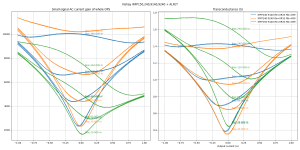
Time for lateral audio MOSFETs! ALF08N16 and ALF08P16.
"Dude these MOSFETS are really fast!" but how much?
Let's look at current gain versus frequency. Yes MOSFETs have current gain just like bipolars, it is basically gm/(jCw). So:

Transition frequency Ft (where gain drops to 1) for the whole push-pull is about 80-120 MHz depending on current. Pretty fast. Another way to look at it is by putting current on the X axis:

This one shows the P and the N (which handle each one sides of the picture) are well matched in speed.
This is at 15V Vce, easy mode for the MOSFETs, so later I will do more measurements at lower Vds.
The relationship between input current and gm is straightforward since they are linked by the input capacitance. I'm including 4 levels of bias, at the same frequency.


These two units are not very well matched, but that should be fixable by playing with source resistors. We'll see if the crossover can be made to look a bit better.
"Dude these MOSFETS are really fast!" but how much?
Let's look at current gain versus frequency. Yes MOSFETs have current gain just like bipolars, it is basically gm/(jCw). So:
Transition frequency Ft (where gain drops to 1) for the whole push-pull is about 80-120 MHz depending on current. Pretty fast. Another way to look at it is by putting current on the X axis:
This one shows the P and the N (which handle each one sides of the picture) are well matched in speed.
This is at 15V Vce, easy mode for the MOSFETs, so later I will do more measurements at lower Vds.
The relationship between input current and gm is straightforward since they are linked by the input capacitance. I'm including 4 levels of bias, at the same frequency.
These two units are not very well matched, but that should be fixable by playing with source resistors. We'll see if the crossover can be made to look a bit better.
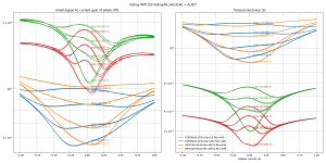
Alright. I've replaced the source resistor on the P-channel with a short, and tried various values for the N-channel: 0R15, 0R33 and 0R47.


Looks like the optimum value for flat gm is between 0R15 and 0R33, and the optimum for current gain flatness around zero would be 0R47.
Here we go, good match in gm with a 0R25 resistor in the source of the NMOS, and a wire in the source of the PMOS.

This won't change the fact that the current gain varies quite a lot however.
Looks like the optimum value for flat gm is between 0R15 and 0R33, and the optimum for current gain flatness around zero would be 0R47.
Here we go, good match in gm with a 0R25 resistor in the source of the NMOS, and a wire in the source of the PMOS.
This won't change the fact that the current gain varies quite a lot however.
Last edited:
The dynamic test gives completely different results from BJTs.
There is no real hFe, so the drive current of the MOSFET is not proportional to the instantaneous value of the output current. Rather it is proportional to Cin*dVgs/dt, which is simply Cin/gm * dIout/dt.
The amusing thing is, for a sinewave output current of a certain amplitude, the drive current always has the same waveform. Its amplitude is proportional to frequency, but its shape does not change.
With BJTs, the drive current is proportional to Iout at low frequency, then becomes ugly as capacitance manifests at medium frequency, then becomes spiky when transit time and other effects screw things up. With these FETs it is much simpler.


There are no spikes. The transient behavior is completely predictable from the parameters extracted from the "transfer function" measurement using the LF and HF sine, since the gm and capacitance parameters do not change with frequency, which only acts as a proportional factor due to the capacitance.
Here on the top graph is the input current at 6kHz. The output current is the blue trace, which is a slow 40Hz with a tiny 6kHz on top. In the total drive current (orange) the 40Hz waveform is barely visible because, due to capacitance, the current for the tiny 6kHz wave is 6000/40=150 times higher. I removed it with a filter to get the drive current for the 40Hz wave, and... it is still exactly the same shape.

Still it would be nicer if these FETs had flatter current gain. I'll see about that, maybe another pair of smaller transistors in parallel to plug the crossover hole.
Phew! Tomorrow I will try IRFP240/9240.
There is no real hFe, so the drive current of the MOSFET is not proportional to the instantaneous value of the output current. Rather it is proportional to Cin*dVgs/dt, which is simply Cin/gm * dIout/dt.
The amusing thing is, for a sinewave output current of a certain amplitude, the drive current always has the same waveform. Its amplitude is proportional to frequency, but its shape does not change.
With BJTs, the drive current is proportional to Iout at low frequency, then becomes ugly as capacitance manifests at medium frequency, then becomes spiky when transit time and other effects screw things up. With these FETs it is much simpler.
There are no spikes. The transient behavior is completely predictable from the parameters extracted from the "transfer function" measurement using the LF and HF sine, since the gm and capacitance parameters do not change with frequency, which only acts as a proportional factor due to the capacitance.
Here on the top graph is the input current at 6kHz. The output current is the blue trace, which is a slow 40Hz with a tiny 6kHz on top. In the total drive current (orange) the 40Hz waveform is barely visible because, due to capacitance, the current for the tiny 6kHz wave is 6000/40=150 times higher. I removed it with a filter to get the drive current for the 40Hz wave, and... it is still exactly the same shape.
Still it would be nicer if these FETs had flatter current gain. I'll see about that, maybe another pair of smaller transistors in parallel to plug the crossover hole.
Phew! Tomorrow I will try IRFP240/9240.
Member
Joined 2009
Paid Member
Lots of interesting data here, not sure I can digest all of it yet!
I would add that I like the sound of ss class ab amplifiers, despite the cross over behaviour. And I have tried cfp in the input, the VAS, the driver and the output. I didn’t like it in the input, or the VAS, yet in those uses it is not switching. I have liked it in the driver and output uses. Still learning!
I would add that I like the sound of ss class ab amplifiers, despite the cross over behaviour. And I have tried cfp in the input, the VAS, the driver and the output. I didn’t like it in the input, or the VAS, yet in those uses it is not switching. I have liked it in the driver and output uses. Still learning!
Yeah that will take some studying lol.
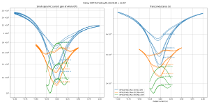
It was a bit cheap of me to test ALFETs at 60mA bias, they deserve a bit more current. I've increased the LF test current to 1A peak, to better show what happens at higher bias.
I've also removed the source resistors completely, because it turns out that the optimum resistor to get a good Gm match depends on idle current. So if it is set for 60mA, it is wrong for 120mA. And these lateral FETs have tempco of the user-friendly polarity, so there is no risk of thermal runaway. Real bias will be a little bit more than what's in the title of the plots though, because without resistors it can't measure the bias, so it's using the same DAC values as in the previous case with resistors.


View attachment 966259
The first one is 60mA bias, second one is 120mA bias, third one is 240mA bias with 1A test current.
So changing the bias simply "stretches" the gm and current gain wingspans, and the bump in the middle goes up at higher bias, just like gm-doubling will do.
There seems to be a loss of gain at high current, too.
One round of applause for AD8421 which did not care and is still measuring current just fine using a piece of wire as a shunt resistor. I couldn't get precision matched wires, and didn't bother calibrating the gain, so the top left graph in the next plot has the wrong scales, of course.
It was a bit cheap of me to test ALFETs at 60mA bias, they deserve a bit more current. I've increased the LF test current to 1A peak, to better show what happens at higher bias.
I've also removed the source resistors completely, because it turns out that the optimum resistor to get a good Gm match depends on idle current. So if it is set for 60mA, it is wrong for 120mA. And these lateral FETs have tempco of the user-friendly polarity, so there is no risk of thermal runaway. Real bias will be a little bit more than what's in the title of the plots though, because without resistors it can't measure the bias, so it's using the same DAC values as in the previous case with resistors.
View attachment 966259
The first one is 60mA bias, second one is 120mA bias, third one is 240mA bias with 1A test current.
So changing the bias simply "stretches" the gm and current gain wingspans, and the bump in the middle goes up at higher bias, just like gm-doubling will do.
There seems to be a loss of gain at high current, too.
One round of applause for AD8421 which did not care and is still measuring current just fine using a piece of wire as a shunt resistor. I couldn't get precision matched wires, and didn't bother calibrating the gain, so the top left graph in the next plot has the wrong scales, of course.
Last edited:
IRFP240/9240 from Vishay are in.
Tested with 0R33 source resistors, and 1A LF current, at 20,60,120mA bias:


Transconductance varies strongly with current (as expected, it's a FET). Current gain at 12kHz and 120mA:
IRFP240/9240 6600-10500
ALFET 8000-14000
A little bit lower than the ALFET, because they have a bit higher capacitance for their gm.
Ft is at least 80MHz at the lowest point at 120mA bias.
At lower bias, the lower current gain means Ft also gets lower.
Everything is much smoother than the laterals which means these are going to generate the least amount of HF distortion.
Matching is pretty good straight out of the box. Both FETs have roughly the same input current versus output current whether they're on or off, which means their input capacitance does not change much with output current. That's nice to know.
Tested with 0R33 source resistors, and 1A LF current, at 20,60,120mA bias:
Transconductance varies strongly with current (as expected, it's a FET). Current gain at 12kHz and 120mA:
IRFP240/9240 6600-10500
ALFET 8000-14000
A little bit lower than the ALFET, because they have a bit higher capacitance for their gm.
Ft is at least 80MHz at the lowest point at 120mA bias.
At lower bias, the lower current gain means Ft also gets lower.
Everything is much smoother than the laterals which means these are going to generate the least amount of HF distortion.
Matching is pretty good straight out of the box. Both FETs have roughly the same input current versus output current whether they're on or off, which means their input capacitance does not change much with output current. That's nice to know.
Last edited:
Hi peufeu,
Interesting results for the IRF9240 which has a "shelf" for gate charge in it's transfer characteristics. I was expecting an input anomaly due to that. High frequencies should have higher driver requirements as well.
This is one pair I would not normally expect to see used as outputs in a high quality amplifier.
Everything is much smoother than the laterals which means these are going to generate the least amount of HF distortion.
Probably, Nelson Pass will agree on this since he favored these HEXFETs on discussions regarding device types.
anatech> Yes, every MOSFET has a shelf in the gate charge plot, this is due to how it is measured as a switch:
The plot shows Vgs in function of gate charge. The FET is wired as a switch with a load resistor at the drain connected to a high Vds.
- It starts with the FET off and Vgs=0
- First the gate charge and Vgs rise until the FET turns on
- When the FET turns on, its Vgs goes down from Vcc to almost zero. During this phase, Vgs stays constant (this is the shelf) because gate current is sucked by Cgd through Miller effect (Vds is moving fast).
- Once it's fully on, Vds is almost zero, and gate current resumes charging the gate capacitance, so the Vgs curve rises again.
That doesn't really apply to a FET in linear mode.
However my measurements are at constant Vgs, which is not exactly like in a real amplifier. When output voltage is low, which is most of the time, Vds is high, so Cgd is low and constant. So it's a good enough approximation. But it says nothing about what will happen when the output gets close to the rails, Vds gets squeezed, and the capacitance changes a lot. I will do that later. If you will, this is more a test about the first few watts of the amp, where there is ample Vce or Vds available.
For now I'm trying to weed out the candidates that will not perform the best at the first watts, because I think this is an important parameter.
Last edited:
Hi peufeu,
That is fair, and a good test. My experience with these comes from their use in Counterpoint amplifiers. The IRF devices are not suitable. That circuit does not use feedback from the output and gate drive is capacitively coupled from a high impedance source. Not an ideal way to drive an output stage.
Really, what happens near clipping isn't a concern as you will have high distortion anyway. That is in support of your point.
-Chris
Probably, Nelson Pass will agree on this since he favored these HEXFETs on discussions regarding device types.
Oh yes, also Mr Pass said source resistors are evil. So, what happens if I put in 1R source resistors to try to make gm more constant, to prevent it from rising so much at high current?
The result is gm-doubling, and it does the same to the current gain.
At 40mA bias it creates a sort of a flat bottom for the gm and gain, but it sharpens the corners, so it isn't good.

At 60mA bias it starts to gm-double, so it will generate more distortion than with the lower resistor value.

At 120mA bias it really gm-doubles hard.

So:
It looks like 0R33 is a good combo, which stays smooth over a wide bias range. At 120mA bias it is really good. This allows an amp with variable bias, for example a "winter" setting and a "summer" setting...
OOPS
The 120mA plot from the previous post was actually 240mA bias, so not comparable. Here's the 120mA bias, with 0R33 resistors, to compare to the plot with 1R resistors in this post.

Also the current sharing plot (top left) is better with the lower resistors. It stays in class A over a wider range of current for the same bias. (this is visible in the 4 corners between the 45° slopes and the horizontals).
Last edited:
Really, what happens near clipping isn't a concern as you will have high distortion anyway. That is in support of your point.
It's important that the amp stay stable... otherwise, yeah, totally agree.
IRFP240+IRFP9140
Since there are way too many plots in this topic, I've put all the curves on top of each other. The color indicates the type of FET, and the bias current is displayed on top. It seems somewhat readable.

Anyway. IRFP9240 and 9140 only makes a small difference, no clear winner. The ALFETs lose both on gm and current gain, though.
Since there are way too many plots in this topic, I've put all the curves on top of each other. The color indicates the type of FET, and the bias current is displayed on top. It seems somewhat readable.
Anyway. IRFP9240 and 9140 only makes a small difference, no clear winner. The ALFETs lose both on gm and current gain, though.
Last edited:
Vishay IRFP150+IRFP9140
IRFP150 has higher gm and lower current gain than 9140 and 9240. It is not a good match.
I've tried an IRFP150 from IR, and the mismatch is even worse. Well, that was expected, 150 and 9140 have very different characteristics.
Unfortunately I don't have IRFP140 to mate with the 9140, and Farnell wants an extra 18€ shipping just for this part, yeah, right.
Attachments
Last edited:
... Counterpoint amplifiers. ... That circuit does not use feedback from the output and gate drive is capacitively coupled from a high impedance source. Not an ideal way to drive an output stage.
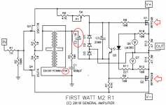
Nelson Pass's First Watt M2 has all of those characteristics. No feedback (anywhere), output MOSFET gates capacitively coupled, output MOSFET gates driven from a 15Kohm output winding on an interstage transformer. Output devices are IRFP240, IRFP9240.
First Watt sold hundreds of them, and the diyAudio Store has sold hundreds more. Owners and builders seem to really love the sonics.
_
Attachments
They don't sound good compared to properly driven outputs. Mind you, the transformer is better than the tube stage use by Counterpoint.
You know, people will buy things that sound awful for various reasons. You'll find that once they are improved those people like them much better. That's as long as you can preserve the overall sonic character and lose the distortion. I am convinced that ad copy is more responsible for satisfaction than listening in these cases.
Note that I am in no way knocking Nelson's products, but I am Counterpoint's amplifier products.
Got a schematic for that Counterpoint? (for the lulz)
FQP3N30/3P20 are in testing.
With the IRFP pair, at a warm but still not unrealistic bias current of about 200mA you get rather constant gm, and constant (and huge) current gain over +/- 1A output current. It's way better than the BJTs. It's way better than I thought.
FQP3N30/3P20 are in testing.
With the IRFP pair, at a warm but still not unrealistic bias current of about 200mA you get rather constant gm, and constant (and huge) current gain over +/- 1A output current. It's way better than the BJTs. It's way better than I thought.
FQP3N30/FQP3P20 is pretty sad...
They have 2x the current gain of the big ones, which means 2x higher Ft, which is nice.
However they want a rather high bias current and low value source resistors to deliver low distortion, but they can't have that... because they're TO220 with rather high RthJC, and a Vbe tempco that is much more cumbersome and runaway prone than the IRFP's...
Attachments
Same story for IRF610/IRF9610.
I thought maybe they would have a properly scaled down version of the big FETs, so using several in parallel would give the same result, only faster. But they don't. The scaling is different between transconductance and thermals. So they want too much bias current for their actual capabilities.
So they are unsuitable for use as output devices in a power amp class-AB output stage (that does not mean they cannot be used for other things, of course).
Attachments
Member
Joined 2009
Paid Member
Topology is key. My TGM8 uses these Hexfet’s in Class C as part of a cfp, whereas my TGM7 (a.k.a. Greg Ball) runs them in rich class AB in common drain. Sounds quite different.
- Home
- Amplifiers
- Solid State
- Power amp OUTPUT STAGE measurements shootout