Like I said earlier something seems amiss with transistor temperatures.
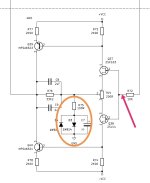
The main PCB is divided in 3 main sections; I assume the bottom two are the L and R line stages, and the top section is made up of the phono stage on the right side, and the final stage of the power supply on the left side. Does that sound right...?
I recorded transistor temperatures, shown in red in the pic below (sorry the writing is not super legible). All are Farenheit and recorded after about 20 minutes running time.

I would have expected temperatures to be somewhat coherent, in the sense that transistors in one channel would run at temperatures roughly similar to their counterparts in the other channel, but as you can see they are wildly different. For instance, the right bank of transistors in the middle section runs twice as hot (232 and 238 F) as the right bank in the bottom section (108 and 110 F).
Also, within the bank of four transistors on the left side of the top section - assuming these are in fact voltage regulators - the bottom two transistors are running roughly twice as hot (156 and 164 F) as the top two transistors (80 and 83 F).
Could this just be a matter of adjusting bias? I count 12 trim pots on this PCB - 4 in each of the 3 main sections - and the heck if I know what they're for. I looked for a service manual or schematics but I was not successful.
As noted before, all heatsink-mounted transistors are Motorola MJF15030 / MJF15031, on both the main and power supply PCBs. I found the original Motorola datasheet (attached). The stated operating temp upper limit is 150 C (302 F).
Interestingly, the Motorola datasheet states: "No Isolating Washers Required", whereas the OnSemi datasheet stays mum on the subject.
What are your thoughts? Bias adjustment? Or...?
The main PCB is divided in 3 main sections; I assume the bottom two are the L and R line stages, and the top section is made up of the phono stage on the right side, and the final stage of the power supply on the left side. Does that sound right...?
I recorded transistor temperatures, shown in red in the pic below (sorry the writing is not super legible). All are Farenheit and recorded after about 20 minutes running time.
I would have expected temperatures to be somewhat coherent, in the sense that transistors in one channel would run at temperatures roughly similar to their counterparts in the other channel, but as you can see they are wildly different. For instance, the right bank of transistors in the middle section runs twice as hot (232 and 238 F) as the right bank in the bottom section (108 and 110 F).
Also, within the bank of four transistors on the left side of the top section - assuming these are in fact voltage regulators - the bottom two transistors are running roughly twice as hot (156 and 164 F) as the top two transistors (80 and 83 F).
Could this just be a matter of adjusting bias? I count 12 trim pots on this PCB - 4 in each of the 3 main sections - and the heck if I know what they're for. I looked for a service manual or schematics but I was not successful.
As noted before, all heatsink-mounted transistors are Motorola MJF15030 / MJF15031, on both the main and power supply PCBs. I found the original Motorola datasheet (attached). The stated operating temp upper limit is 150 C (302 F).
Interestingly, the Motorola datasheet states: "No Isolating Washers Required", whereas the OnSemi datasheet stays mum on the subject.
What are your thoughts? Bias adjustment? Or...?
Attachments

Haven´t seen the schematic´s, this is of course just a guess.....What are your thoughts? Bias adjustment? Or...?
but having 4 trimmers in each section could be (assuming balanced) 2 for bias and 2 for DC-balance.
If so, and when you find out which is which, then I would find the resistor(s) going to collector (or emmitter depending on circuit),
and measure voltage across it (on the "hot side"/channel) and compare with the same resistor(s) on the "cold side"/channel, and adjust
the "hot one" to the same value as the "cold one" ???
I´ll take a read again and see, if you provided the schematic somewhere (I don´t remember)
@Boydk I do not have schematics unfortunately. I did search
@Simon1972
Would you happen to have schematics from the time you refurbished your KSP-7B by any chance?
@Simon1972
Would you happen to have schematics from the time you refurbished your KSP-7B by any chance?
Hi MFRD,
Earlier Krell pre-amps used Supertex VN0206/ VP0206 output transistors. Actually with 0.33R source resistors. I would guess that the trimmer closest to heatsink is the bias adjustment.
If you took a bunch of close-up photos of both PCB sides, I think we would be able to reverse the circuit and draw a schematic.
Those numbers to me are crazy hot. Tj is be spec'ed at 150, not case temp. And that is the absolute maximum which anything above is destructive. Me, I never run over 100C case, and even that is iffy. I think expected life is halved for each 10C increase in temperature, and many devices are spec'ed to only 70C. I also ran some numbers assuming an 11C/W thermal resistance for the heat sink which is a wag at a TO220 heatsink like the one in the photo. Assuming 25C room temp, for each device, leaving out the two devices 80/83F, I get
156F DT 46C 4.2W
164F DT 46C 4.2W 8.4W
109F DT 17C 1.5W 9.9W
238F DT 89C 8W 18W
107F DT 17C 1.5W 19.5W
145F DT 37C 3.3W 22.8W
232F DT 86C 7.8W 30.6W
108F DT 17C 1.5W 32.1W
145F DT 38C 3.5W 35.6W
110F DT 18C 1.6W 37.2W
which seems reasonable as consumption is 44W leaving around 6W for the non-heat sinked circuitry. The 238 device is probably near self destruct if my numbers are in the ballpark. 238F is 114C, and with thetaJC of 3.5C/W @ 8W adds another 28C between case/junction to get a junction temp of 142C,a mere 8 degrees shy of destruct. No way Krell designed it that way. As you note, the asymmetry in the temps says something is wrong. Maybe trimpots went open on one channel, easy to check first.
Hi folks, here are hi res pics of the top and bottom layers of one channel section (the "bottom" section on the whole-PCB pic). The pic of the bottom layer is flipped horizontally,
![line stage section [top layer].jpg](https://www.diyaudio.com/community/attachments/line-stage-section-top-layer-jpg.1441911/ "line stage section [top layer].jpg")
![line stage section [bottom layer].jpg](https://www.diyaudio.com/community/attachments/line-stage-section-bottom-layer-jpg.1441912/ "line stage section [bottom layer].jpg")
As @mkc said the source resistors are .33 ohm (all 8 measure correctly).
The 4 trim pots located closest to the heatsinks are 5K ohm (VRN 752-208).
They're wired as variable resistors (wiper connected to ground).
@mikeAtx I did measure them - 512, 530, 570 and 718 ohm so they're not open, but don't these values seem really low with respect to their 5K range? You'd think they'd use 1K ohm pots if they only plan to set them at a few hundred ohms?
The trim pot that reads highest - 718 ohm - is the one connected to the bank of overheating transistors.
The other 4 trim pots are VRN 752-208 too, but 200 ohm. They're wired as pots. They're set near their midpoints, 90-100 ohm or so.
Hi @MFRD,
Could you please list the small-signal transistors? I earlier pre-amps Krell used 2SC2240BL/2SA970BL and jfets like 2SK163/2SJ44. But, as you state the output transistors are all bipolare, they might use something completely different. They have been known to use A42/A92. Do they use those here?
Could you please list the small-signal transistors? I earlier pre-amps Krell used 2SC2240BL/2SA970BL and jfets like 2SK163/2SJ44. But, as you state the output transistors are all bipolare, they might use something completely different. They have been known to use A42/A92. Do they use those here?
@MFRD
Sounds like you´re on to something here.
The 5K pots are surely the bias pots, and the 200R pots most likely DC adjust.
The bias pots could easily have burn-spots, so replace them all. Nothing wrong with replacing them with 1K or 2K, since you now know,
that reasonable bias can be achieved within 500R or so.
I would (probably) measure the voltage across the bigger 680R resistors close to the front of the transistors/heatsinks. If it´s higher on the "hot one",
You´ll have some pointers to adjust by.
Set the pots to f.ex. 400R to begin with, and adjust them all to give the closest result to the "cold" one.
Then adjust the 200R´s for minimum DC out 😉
@MFRD
First draft attached. Please take with a grain of salt. Mistakes are likely. And there are some missing values and designators are not matching the actuall PCB. Not all are vissible on the PCB.
This is an old preamp so I don't know if there is any issues with copyright. If so, moderators may have to delete my post.
Now, if you could take some pictures of the phono section we might also document that 🙂
Attachments
EDIT:
For some stupid reason (late night, missing glasses) 🤣 🤣
I missed the "big" 0R33´s (emitter resistors on the output´s). Probably better to measure across those.
You´ll probably only read a few milliVolts, but adjust the "hottest" to match the coldest.
If you want to down adjust further, put a scope on the outputs, and make sure, there´s no crossover distortion.
This should help you run the pre as cool as possible.
Last edited:
@mkc
Thank you so much for drawing this draft schematic, that is very helpful!
I was thinking about the question of copyright earlier, in reference to cloning the power supply board.
In doing so I would essentially be making a copy of a PCB that purports to be protected by copyright (let's assume that it is so, for argument's sake). It is part of a 34-year old piece of equipment that is no longer serviced by its manufacturer, which is not engaged in business at this point in time.
I believe that under US law, my copy / clone is permitted under Fair Use, the doctrine that permits a person to make a copy of a movie or a LP that they already own for personal or archival purposes.
In addition, many US states have passed Right to Repair laws that give owners broad rights to maintain and repair their gear. Interestingly, these laws were pioneered by a handful of YouTube repair channels. These laws deserve to be better known.
Take the above with a grain of salt. It's just the uninformed musings of a non-lawyer 🙂
I was thinking about this one some more having seen this pulls a little over 1A at steady state.
You could potentially consider a Smooth Like Buttah' Power Supply. I imagine most of these are in power amps, but a preamp pulling 50W could be a good application for SLB. Put it in a ventilated box and make sure there is enough chassis metal to act as a heatsink for the CapMx semis.
You could potentially consider a Smooth Like Buttah' Power Supply. I imagine most of these are in power amps, but a preamp pulling 50W could be a good application for SLB. Put it in a ventilated box and make sure there is enough chassis metal to act as a heatsink for the CapMx semis.
Edit July 28, 2023: here are the schematics, BOM, and info on the single rail SLB. https://www.diyaudio.com/community/...x-class-a-power-supply-gb.336479/post-5782376
Edit Jan 23, 2020: Connection diagram for single trafo and dual rail SLB with M2X amp
The SLB (Smooth Like Butter) Active Rect/CRC/Cap Mx Class A Power Supply GB
Edit June 16, 2019: Error on Q5 orientation on Single Rail (SR) board. Please install Q5, BD139 with pin 1 to the square pad (as customary) but this will have front of part in contact...
- xrk971
- Replies: 1,756
- Forum: Group Buys
@rhthatcher
Funny you should mention the SLB, I was reading that thread recently and I was thinking it would be a pretty good match for the Krell.
Do you have experience with the SLB?
It is said to run cool. Presumably even more so driving the Krell, I guess. That's good.
At this point I am pretty much set on working with the Krell case, for originality's sake. Yes, I know it's poorly designed in every which way.
I'm not against putting a better PSU inside it, if feasible. I'm not finding the SLB's dimensions though. Guess I'll head over there and ask.
All that said, he does seem to be out of the dual rail PCB.
I’ve used the SLB in a power amp - it’s a really nice design. Drop him a direct message about stock. If his online store inventory quantities are anything like my Etsy store - he may have some boards hanging around.
- Home
- Design & Build
- Parts
- Please wake me up from this PCB nightmare [Krell KSP-7B Power Supply]