If you have to go differential, you better forget discrete circuits. Matching discrete parts is out for us mere mortals. Too many to measure and match a few pairs.
The problem with ICs is mostly implementation and power supply related. Parts quality too.
The problem with ICs is mostly implementation and power supply related. Parts quality too.
I'm not happy with digital recordings, but why make things even worse?
If I'm going to use differential signal from the dac than I don't need inverting IC, only buffer on the cold input?
Your last simulation was with buffer addition? Is it too good to post it here?)
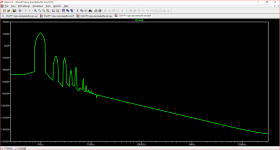
The simulation I did for the FFT in post 213 was with signal sources generated within SPICE so there was no buffer involved.
Anyway I have simulated the circuit with an LT1010 buffer IC to show what effect introducing this would have on the results. It looks tidier to me - I have attached the simulation file and FFT for your information.
It is notable that the most prominent harmonics are second and third in declining proportion regardless of the presence of an IC op.amp in the circuit see LT1010 - Fast 150mA Power Buffer - Linear Technology for more detail.
The simulation file is configured for a normal unbalanced input signal input which is the most simple route for you to take to get your amplifier working.
If you download SPICE in the first instance and then the .asc attachment you will be able to run the simulation by right clicking on the image. If you put the cursor over the circuit there will be a reading at the bottom left hand corner of the file. The dc offset is 9 mV and the Iq in the output transistors is 18 mA each.
The 1kHz THD is 0.0041% in theory which would seem optimistic when you look at the LT1010 data in the link.
Attachments

The simulation I did for the FFT in post 213 was with signal sources generated within SPICE so there was no buffer involved.
Could you please describe how to simulate the schematic with balanced signal source with FFT, as you did in post 213?
Do you know how to integrate to the schematic I'm using the buffer with 4 transistor arrangement of Q31, Q32, Q35, Q36 from Dadod schematic?
Thanks.
Last edited:
You could take Dadod's circuit as illustrating an idea. It is not too different from a circuit I used a long time ago and I have simulated this in anticipation of your asking this question.
As a first step I simulated this on its' own with a 600R load which is about as much as it will tolerate - THD with this load is worse than with LT1010 in the main circuit.
If that part is replaced by the discrete buffer in the main circuit THD increases to 1.4%
If you look at dadod's buffer you will see an 820R buffer resistor in series with the output which indicates the loading is not so demanding.
I am attaching the revised simulation with the discrete buffer and the FFT.
There is no point in simulating a balanced line to unbalanced until the buffer stage is sorted out.
Attachments
Here is the discrete buffer on it's own - it will be easier to test this. Looking at this again with 600R the THD is a little better than with LT1010 in the main circuit unfortunately with the load imposed on the discrete buffer in the main circuit it does not have the grunt.
Sorry about that - the .asc file keeps shrinking to the size of a postage stamp when changing screens which makes it harder to keep track of the work.
Sorry about that - the .asc file keeps shrinking to the size of a postage stamp when changing screens which makes it harder to keep track of the work.
Attachments
Last edited:
If that part is replaced by the discrete buffer in the main circuit THD increases to 1.4%
If you look at dadod's buffer you will see an 820R buffer resistor in series with the output which indicates the loading is not so demanding.
I am attaching the revised simulation with the discrete buffer and the FFT.
There is no point in simulating a balanced line to unbalanced until the buffer stage is sorted out.
As for me it looks pretty the same in term of noise with different signature.
On Dadod's schematic and as Keantoken advised, there is only the need of buffer on negative input. You applied it to both hot and cold inputs. Is it really necessary? Why don't you use voltage supply from amplifier front end? Discrete parts (bc550\560) have much higher tolerances than 15V with possible benefit of lower distortion.
You wrote in post 213 you simulated the amplifier with a balanced signal input, you corrected without buffer. I don't understand, why it didn't work before, when you said there is a hiatus in simulation at the midpoint?
If the amp works without buffer if feeded with differential signal, perhaps there is no need for any buffer. If we want to use SE input, we may "turn off" cold input transistors or feed the signal to hot input only with cold one left floating.
Dear AndriyOL,
While I love your enthusiasm for SSA derived amps (which I share) I would advice against the path you are following now and recommend you follow the several good advices that our more knowledgeable mates are giving in relation of the best strategy to follow to have the most important: first a functionally stable amp.
It is very brave to want to end up with the best amplifier possible at first attempt but the challenge is proving very hard and you may get discouraged after several frustrating tries... 😱
I recommend:
1) you make the unbalanced input version and get it stable in all conditions first.
(BTW, it seems unwise to "let floating the cold input", without referring it to ground, as the unstable amp could make all sort of bad things, even kaput)
2) when you have the unbalanced amp OK, you may add some sort of bal/unbal converter like an input transformer or a THAT chip receiver (which was designed by a TX expert, as I remember) which will give you excellent performance, OR,
3) use two amplifiers in balanced configuration to drive one speaker, a plan that I will love to do in the future as I own balanced sources and volume controls...
My knowledge is far inferior than that of the previous contributors but my recommendations go with all my best wishes to you.
Cheers,
M.
PS: shorten and twist all power supply and signal cables. 😉
As for me it looks pretty the same in term of noise with different signature.
On Dadod's schematic and as Keantoken advised, there is only the need of buffer on negative input. You applied it to both hot and cold inputs. Is it really necessary? Why don't you use voltage supply from amplifier front end? Discrete parts (bc550\560) have much higher tolerances than 15V with possible benefit of lower distortion.
You wrote in post 213 you simulated the amplifier with a balanced signal input, you corrected without buffer. I don't understand, why it didn't work before, when you said there is a hiatus in simulation at the midpoint?
If the amp works without buffer if feeded with differential signal, perhaps there is no need for any buffer. If we want to use SE input, we may "turn off" cold input transistors or feed the signal to hot input only with cold one left floating.
To answer your last question proceed as follows.
Download SPICE and when you have this installed click on the attachment I posted.
This will automatically prompt you to open SPICE.
Then looking at the toolbar at the top you will see a arrow pointing anti-clockwise to undo any changes you make
Next' click on the scissor tool and snip the line from the buffer output and right click on anywhere on the schematic.
From the drop down menu select Run.
A black cross (as in sighting a target) will appear.
Use your mouse to move this to touch the output - a red probe will appear - right click on this.
This will open a separate half window showing the output signal plot.
Right click with your mouse anywhere in the separate section
From the drop-down menu that appears select the option at the bottom of the list "View".
Right click on the first option FFT this will open a new window showing V(vout) already selected - this corresponds with the label attached to the output in the schematic.
In the field "Time range to include" left click on ''specify a time range" the end time is already specified - enter 4ms in "Start Time" and right click on "OK". You will then see the display in the plot window.
Right click on the plot window and from the drop down menu go to the bottom option again "View" and select the option "SPICE Error Log"
This will open a small window on the screen - scroll to the bottom where the "Total Harmonic Distortion" percentage is shown.
Exit that screen and maximise the schematic. Use your mouse to touch the amplifier output and read the dc offset result at the left on the bar at the bottom of your screen.
The current through resistor will show in that space if the mouse hovers overhead - a symbol with a red arrow will appear when on target. Use this to check the output transistor current. This will tell you something about Iq if not the levels under dynamic conditions.
If you want to keep a record of this save the file under a new name. Close the one in use and select the "No" option on the question of saving changes to my attachment.
(BTW, it seems unwise to "let floating the cold input", without referring it to ground, as the unstable amp could make all sort of bad things, even kaput)
Thank you for your best wishes and recommendations Maxlorenz.
When I ground cold input, the appropriate input transistors are getting biased with 1\3 more current than if left floating.
I think it's pointless to use bal amplifier input with bal\unbal inverter without ability to accept diff input signal. In that case I can design pcb from already proved working SE SSA schematic.
I don't need fully balanced circuit, it wouldn't be good costwise. Just the amp with ability to accept diff signal and a benefit of not being prone to pick up noise.
To answer your last question proceed as follows
Thanks Mjona, I've got the picture now.
I tried to do the same with balanced signal input without buffer but the result was with 30% thd. How did you do this in post 213?
Last edited:
Thanks Mjona, I've got the picture now.
I tried to do the same with balanced signal input without buffer but the result was with 30% thd. How did you do this in post 213?
I did this using the signal generators in SPICE which do as they are told.
The input impedance of a power transistor is low and to drive them to capacity would require quite a lot of current.
In post 207 keantoken observed the input signal at the inverting input would see a load of 100R in the feedback path R17-R2 and R18-R4.
The amount of current drive for the purpose can be seen by those passed for instance through R2 and R4 in the attachment.
An LT1010 is a capable real life substitute for the SPICE generator - for a discrete transistor circuit you will need something better than the simple one I posted.
Attachments
Thank you for your best wishes and recommendations Maxlorenz.
I think it's pointless to use bal amplifier input with bal\unbal inverter without ability to accept diff input signal.
In that case I can design pcb from already proved working SE SSA schematic.
An input transformer or a balanced line receiver will accept differential signal. I don't understand what you mean...quality ones will have way better CMMR than that you can achieve with discrete input. SSA has only 10K impedance...one could modify the input to work with JFETs but it would be probably too complicated. I attached PDF about THAT 1200 line of balanced receivers, designed by Bill Whitlock from Jensen Transformers (!) where a complete analysis of the problem is described, for those interested...
This topic of oscillations is fascinating, but it is, I imagine, one of the toughest problems you can find, even for advanced students of the art...
Having faced it a couple of times recently, I luckily solved them.
May I make a question for The Wise?
This current feedback amp is fast and has apparently extended frequency response (not 80MHz, I hope!), but not as fast as its feedback, or so I was inclined to believe...
What would be the effect of, once having chosen the perfect value for R feedback, to swap it for equivalent, high quality, non inductive, in series chain of resistors?
Would it make the amp more stable of more prone to oscillation???
Thanks,
M.
Attachments
Distortion should go down, because voltage coefficient divided by resistors number (but only for the amp with very low distortion otherwise hidden) and it should be stable (even with longer NFB path) if the amp had enough PM and GM previously with one resistor.What would be the effect of, once having chosen the perfect value for R feedback, to swap it for equivalent, high quality, non inductive, in series chain of resistors?
Would it make the amp more stable of more prone to oscillation???
Thanks,
M.
Actually I made provision in my CFA to swap paralleled resistor with the series chain of resistor but not tried it yet.
Distortion should go down, because voltage coefficient divided by resistors number (but only for the amp with very low distortion otherwise hidden) and it should be stable (even with longer NFB path) if the amp had enough PM and GM previously with one resistor.
Actually I made provision in my CFA to swap paralleled resistor with the series chain of resistor but not tried it yet.
Great!
Thank you very much.
M.
I tried the same but without success. Could you please show the asc file?I did this using the signal generators in SPICE which do as they are told.
The amount of current drive for the purpose can be seen by those passed for instance through R2 and R4 in the attachment.
An LT1010 is a capable real life substitute for the SPICE generator - for a discrete transistor circuit you will need something better than the simple one I posted.
That amount of current for the purpose to drive power transistors is 5mA or 18mA? How should it be seen from the attachment? As far as I know possible limit through R17, R18 is 4-4.5mA.
In addition, LT IC will require third PSU which is not practical.
Dadod's buffer from the schematic can't be implemented or it doesn't comply with the purpose?
Last edited:
An input transformer or a balanced line receiver will accept differential signal. I don't understand what you mean...quality ones will have way better CMMR than that you can achieve with discrete input. SSA has only 10K impedance...one could modify the input to work with JFETs but it would be probably too complicated. I attached PDF about THAT 1200 line of balanced receivers, designed by Bill Whitlock from Jensen Transformers (!) where a complete analysis of the problem is described, for those interested...
This topic of oscillations is fascinating, but it is, I imagine, one of the toughest problems you can find, even for advanced students of the art...
Having faced it a couple of times recently, I luckily solved them.
May I make a question for The Wise?
M.
Such transformers are very expensive and have a very limited bandwidth, not worth a try.
My fault, I didn't understand you first, sorry.
Does CMRR matters much? Differential signal isn't amplified in this circuit separately.
What could be a benefits using JFETs here?
Thanks, I'll read it.
I guess your question is not addressed to me)
Regards.
Distortion should go down, because voltage coefficient divided by resistors number (but only for the amp with very low distortion otherwise hidden) and it should be stable (even with longer NFB path) if the amp had enough PM and GM previously with one resistor.
Actually I made provision in my CFA to swap paralleled resistor with the series chain of resistor but not tried it yet.
Do you guys have an equipment to measure real amp distortion? Would be interesting to know the comparison results.
Last edited:
Does CMRR matters much? Differential signal isn't amplified in this circuit separately.
What could be a benefits using JFETs here?
Well, the whole point of having diferential input is avoiding picking-up noise in noisy environment, right? It is not done because it is cool...the noise picked-up will be common to both signal cables, am I right?
The article is very illustrative and THAT chips are cheap enough, way cheaper than a good Tx.
Cheers,
M.
I tried the same but without success. Could you please show the asc file?
That amount of current for the purpose to drive power transistors is 5mA or 18mA? How should it be seen from the attachment? As far as I know possible limit through R17, R18 is 4-4.5mA.
In addition, LT IC will require third PSU which is not practical.
Dadod's buffer from the schematic can't be implemented or it doesn't comply with the purpose?
The .asc file is attached. See also the second attachment -in the tool needed for a signal generator has a green blob below. Left clicking opens the less common components elsewhere on the tool bar. Scroll across the right and click on "voltage" and the symbol will appear click on OK - you can drag one and left click at a place desired in the schematic. You can have as many as you like by repeat left clicks - here you need only one - right click to exit.
Moving the cursor over the created symbol will bring up a symbol with a pointing white hand - right click over this brings up the fields needing to be entered - I copied these from V3 and clicked OK.
After that process hovering over a component will bring up the symbol with the red arrow.
In the same attachment there is a red circle around the tool used to plot such parameters as V[vin] etc V[vout] [n001] I[C1], I[R1], I[V1] Ib[Q1], etc,etc.
You can use these to see what happens under dynamic conditions - and there is much more scope to explore what is happening at various points of the circuit.
On the question of dadod's buffer it is entirely suited for his purpose. In this circuit there is a snag in that dadod's needs a buffer resistor at the output of 820R.
You can test what would happen in your circuit by right clicking on the resistor symbol in the tool bar, and left clicking and dragging this into place in the connection between V4 and the inverting input. Move the cursor to hover and enter 820 in the resistor value field and click Ok.
Right click on the schematic and select Run and follow the steps previously outlined for FFT and SPICE Error Log.
Attachments

I just realised that model for the LT is not included in the simulation. For anyone unfamiliar with SPICE this and the voltage supply symbols for this will have to be snipped out or else there will be an error message.
I have revised the simulation for the circuits 1. with LT1010 as the buffer - as it turns out this is in library and 2. with a revised version of the 4 transistor buffer which gets close to this in performance using higher voltage rails available within the amplifier some resistor value changes and higher voltage transistors.
With a test load included in the simulation the respective figures for THD at 1kHz are 0.0042% and 0.0056%.
The 4 transistor buffer could be further tuned with different resistor values as long as transistor dissipation is less than 600 mW - one could try replacing these with some of those used in the main power amplifier. Hover over the transistor of choice and copy the name - then hover over whichever of the four transistors to open the dialogue box and paste. The dissipation will register with the white hand pointer symbol moving over the transistor - read this in the left side of the bar at the bottom of the .asc screen.
Attachments
- Home
- Amplifiers
- Solid State
- One of the Top Solid-State CFA amp design