Many thanks for your detailed explanation, I appreciate this.
I tried to simulate without LT IC or descrete buffer and got 0.0037% THD, but than noticed you set positive signal source for both hot and cold input of the amp. Doesn't it has to be negative signal source to cold input? With negative signal source to cold input I'm getting 30% THD.
With LT IC or descrete buffer this is only SE input, according to the schematic?
Yes, you are right about noise. What do you mean by -it is cool?
I tried to simulate without LT IC or descrete buffer and got 0.0037% THD, but than noticed you set positive signal source for both hot and cold input of the amp. Doesn't it has to be negative signal source to cold input? With negative signal source to cold input I'm getting 30% THD.
With LT IC or descrete buffer this is only SE input, according to the schematic?
Well, the whole point of having diferential input is avoiding picking-up noise in noisy environment, right? It is not done because it is cool...the noise picked-up will be common to both signal cables, am I right?
Cheers,
M.
Yes, you are right about noise. What do you mean by -it is cool?
Attachments
Last edited:
Be aware there have been a couple of key changes to the circuit in the simulation by keantoken - previously seen by r_merola in his post 78 on page 8.
The changes involve Q8 and Q9 where the collector and emitter connections were reversed in the original circuit so you need to check your board to see if the overlay follows the original circuit which has them the wrong way around or the simulation on the other hand.
Correctly oriented Q8 and Q9 the collector loads their configuration changes these to common emitter amplifiers which invert the phase of the drive at the junction of the collector and load.
As the result of this the amplifier simulation requires a different phase input at the - input. In the wrong configuration the simulation bears some resemblance to what you have seen on your scope.
Last edited:
if there was ever an award for the most altruistic work put in to help a distant stranger - mjona - you'd get my vote!
if there was ever an award for the most altruistic work put in to help a distant stranger - mjona - you'd get my vote!
Cheers for that
Be aware there have been a couple of key changes to the circuit in the simulation by keantoken - previously seen by r_merola in his post 78 on page 8.
The changes involve Q8 and Q9 where the collector and emitter connections were reversed in the original circuit so you need to check your board to see if the overlay follows the original circuit which has them the wrong way around or the simulation on the other hand.
Correctly oriented Q8 and Q9 the collector loads their configuration changes these to common emitter amplifiers which invert the phase of the drive at the junction of the collector and load.
As the result of this the amplifier simulation requires a different phase input at the - input. In the wrong configuration the simulation bears some resemblance to what you have seen on your scope.
Keantoken said it was his mistake in CCS transistors orientation. However simulation works better without buffer with "wrong" oriented CCS transistors, if I'm not mistaken.
What should I notice? Very small power dissipation and current consumption?Notice anything about Q6 and Q7 in the simulation?
Attachments
Last edited:
Keantoken said it was his mistake in CCS transistors orientation. However simulation works better without buffer with "wrong" oriented CCS transistors, if I'm not mistaken.
What should I notice? Very small power dissipation and current consumption?
I looked at the corrected configuration by keantoken with the CCS shown correctly - this involved changing the connections for Q6,7,8 and 9.
The original schematic you posted showed these the wrong way around along with the board layout. If you got these two items from the same source there is a question as to whether or not the board reflects the errors in the picture.
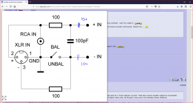
There are a couple of things that obstructed progress in getting this circuit sorted if the circuit is to be operated with the option of balanced or unbalanced input.
The first of these is that there the signal input to the - or cold terminal needs a capacitor in the feed line. This and that in the hot feed line are parts that I added to keantokens simulation.
I mentioned in post 186 that lowering supply line voltage would affect Q16 Miller capacitance. I see the compensation for the Vas transistors Q16 see C34 see Q17 C35 has been attended to by reducing the capacitor values from 50 pF to 8 pF along with some fine tuning to some other small capacitor values elsewhere.
This has eliminated a hidden phase anomaly insofar as balanced input was concerned. I was not planning to do a square wave test until later - my wife has had an accident and I am taking her to hospital this morning.
I ran the new simulation with the inverting signal input - the circuit seems to run equally well whatever the input signal phase is and if the inverting signal input is grounded as well.
In all cases there must be a capacitor between the cold input and the signal generator or ground.
According to the simulation a direct connection results in no sine wave only the dc offset - see more on this later. This is a bit worrying since you mentioned earlier that grounding direct caused the output stage to run hot!
Capacitors C25 and C26 are added parts to the simulation that will need to be fitted in your hardware.
There was a recommended switchable XLR connection for this circuit.
I have attached this and a copy of the original circuit with some notes on changes between this and the latest simulation.
Check this against the simulation to see that there are no other changes that I might have missed.
I recommend scrutinizing the board to see that the transistor connections line up with what the latest simulation indicates.
The new simulation dc offset is -2.2 volts and the output Iq is low but leave that until you have checked the board.
Attachments

I'm writing this post a third time already, it keeps deleting in the middle of my answer and I have to start again.The original schematic you posted showed these the wrong way around along with the board layout. If you got these two items from the same source there is a question as to whether or not the board reflects the errors in the picture.
I mentioned in post 186 that lowering supply line voltage would affect Q16 Miller capacitance. I see the compensation for the Vas transistors Q16 see C34 see Q17 C35 has been attended to by reducing the capacitor values from 50 pF to 8 pF along with some fine tuning to some other small capacitor values elsewhere.
This has eliminated a hidden phase anomaly insofar as balanced input was concerned. I was not planning to do a square wave test until later - my wife has had an accident and I am taking her to hospital this morning.
I ran the new simulation with the inverting signal input - the circuit seems to run equally well whatever the input signal phase is and if the inverting signal input is grounded as well.
According to the simulation a direct connection results in no sine wave only the dc offset - see more on this later. This is a bit worrying since you mentioned earlier that grounding direct caused the output stage to run hot!
Check this against the simulation to see that there are no other changes that I might have missed.
I recommend scrutinizing the board to see that the transistor connections line up with what the latest simulation indicates.
The new simulation dc offset is -2.2 volts and the output Iq is low but leave that until you have checked the board.
What original schematic do you refer to, in 1 post, in post 180 or my latest SSAHP kplus dual siggen sim2 file? Are you saying the CCS transistors in post 180 were connected in a wrong way? My board layout is the same as the schematic in post 1 regarding CCS connection.
I was testing the amplifier with 4.5uF input capacitors. I've changed the compensation capacitors to 8pF following Johnego advices regarding multipole compensation. After that there are almost zero oscillations on the outputs, only some left on front end supply rails. But I still haven't figured out why they appear and how to eliminate them. That's why I gues the amp is not stable at cold start.
So, the amplifier can work now with balanced inputs as is and without the buffer, according to simulation (as you understand it better than me)?
I mentioned before that when grounding cold input there was significant input LTP transistors bias current increase from 3.3mA to 3.9mA, the output was not affected.
DC offset depends on balance set by R8, R9 pots. I left the current values 43\45R, as the simulation thd was a bit better.
I noticed you changed R37, R38 in Vbe multiplier schematic. This change should increase output bias current, if I'm not wong?
I changed the R9, R8 to 42\56R and the offset is 36mV. In fact I have them 44\45R with zero offset.
Later this week I'll accomodate CCS ransistors change on the boards and let you know.
I wish your wife to have a quick recovery. Take care yourself and family.
Thanks and with Best regards.
Andriy.
Last edited:
Thank you guys. We are learning a lot here.
Is Spice able to calculate CMRR for this balanced input section, taking into account parts tolerances, etc...?
Best wishes to Mjona.
M.
Is Spice able to calculate CMRR for this balanced input section, taking into account parts tolerances, etc...?
Best wishes to Mjona.
M.
I'm writing this post a third time already, it keeps deleting in the middle of my answer and I have to start again.
What original schematic do you refer to, in 1 post, in post 180 or my latest SSAHP kplus dual siggen sim2 file? Are you saying the CCS transistors in post 180 were connected in a wrong way? My board layout is the same as the schematic in post 1 regarding CCS connection.
I was testing the amplifier with 4.5uF input capacitors. I've changed the compensation capacitors to 8pF following Johnego advices regarding multipole compensation. After that there are almost zero oscillations on the outputs, only some left on front end supply rails. But I still haven't figured out why they appear and how to eliminate them. That's why I gues the amp is not stable at cold start.
So, the amplifier can work now with balanced inputs as is and without the buffer, according to simulation (as you understand it better than me)?
I mentioned before that when grounding cold input there was significant input LTP transistors bias current increase from 3.3mA to 3.9mA, the output was not affected.
DC offset depends on balance set by R8, R9 pots. I left the current values 43\45R, as the simulation thd was a bit better.
I noticed you changed R37, R38 in Vbe multiplier schematic. This change should increase output bias current, if I'm not wong?
I changed the R9, R8 to 42\56R and the offset is 36mV. In fact I have them 44\45R with zero offset.
Later this week I'll accomodate CCS ransistors change on the boards and let you know.
I wish your wife to have a quick recovery. Take care yourself and family.
Thanks and with Best regards.
Andriy.
Thanks she has a broken arm in a sling it takes 6 weeks for breaks to heal. I am retired and - handling the domestic tasks in this short term will simply mean less time for recreational pastimes.
I looked at the orientation of the CCS transistors on your pcb. As you have seen this is accord with the schematic in the attachments to posts 1 and 180 - whereas these transistors need to be as per the orientation in your latest simulation.
The in line disposition of the leads of the 2SAXXX and 2SCXXX and the collector in between the base and emitter will require some improvisation to transpose the collector and emitter connections on your pcb.
There might be a need to change some trimpot values if those don't allow enough adjustment or if there is difficulty in pinning down output transistors Iq and dc offset.
There are two aspects of the implementation to query - first there is no provision for any fuses on the board between the power amplifier sections and the supply capacitors. Secondly to set the output Iq for low THD the voltage drop across the emitter resistors needs to be 27 mV - rule of thumb.
To achieve that with three output sets, the total Iq using 0.1 Ohm emitter resistors will result in a lot of heat.
To me neither of these things make a lot of sense - if your amplifier fails and goes dc this could set fire to your speakers and even cause a house fire.
Thank you guys. We are learning a lot here.
Is Spice able to calculate CMRR for this balanced input section, taking into account parts tolerances, etc...?
Best wishes to Mjona.
M.
Try this link YouTube
There are two aspects of the implementation to query - first there is no provision for any fuses on the board between the power amplifier sections and the supply capacitors. Secondly to set the output Iq for low THD the voltage drop across the emitter resistors needs to be 27 mV - rule of thumb.
To achieve that with three output sets, the total Iq using 0.1 Ohm emitter resistors will result in a lot of heat.
To me neither of these things make a lot of sense - if your amplifier fails and goes dc this could set fire to your speakers and even cause a house fire.
There are 15A smd fuses on the pcb near voltage terminals.
As far as I know optimal voltrage drop on 0.1R Re for best performance is 16-18mV which equals 160-180mA of bias current.
Of course there should be some kind of DC sense, soft start, overcurent protection.
I tried to simulate with 20K sine on inputs but distortion resulted very high. Am I doing something wrong?
Last edited:
There are 15A smd fuses on the pcb near voltage terminals.
As far as I know optimal voltrage drop on 0.1R Re for best performance is 16-18mV which equals 160-180mA of bias current.
Of course there should be some kind of DC sense, soft start, overcurent protection.
I tried to simulate with 20K sine on inputs but distortion resulted very high. Am I doing something wrong?
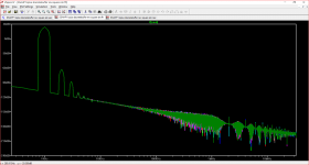
My simulation of your model gives 0.0046% THD at 20 kHz and the FFT shows the fundamental and second and third harmonics declining in a nice pattern.
At a practical level if you run your amplifier with 160 -180 mA per output transistor set your total Iq will be of the order of .5 A which will generate a considerable amount of heat.
Bob Cordell made a SPICE tutorial available on his website and output stage dissipation is one of a number of amplifier tests he devised that you can investigate further at CordellAudio.com - Tutorial Simulations
If you intend running .5 A of output Iq the requirement for heat sinks and power transformer rating will need to be more substantial.
Can you give some details for these.
In the original circuit the work of a well accomplished contributor on this site the value of the output transistor emitter values were 0R22. That much you should stick with.
As a matter of interest I found that increasing the emitter resistors to 0R47 and reducing the total Iq to .18A or 180 mA resulted in no significant change in the THD - new .asc file attached.
Attachments
If you intend running .5 A of output Iq the requirement for heat sinks and power transformer rating will need to be more substantial.
Can you give some details for these.
In the original circuit the work of a well accomplished contributor on this site the value of the output transistor emitter values were 0R22. That much you should stick with.
As a matter of interest I found that increasing the emitter resistors to 0R47 and reducing the total Iq to .18A or 180 mA resulted in no significant change in the THD - new .asc file attached.
In the sim file the SINE frequency on both inputs is 1KHz. When I tried to change it to 20K I got 70% THD.
I remade the pcb to the CCS transistors change according to the latest simfile. As on simulation I have 2.5V DC on output, other channel 0.5V and i can't set it to zero, changing pots resistance doesn't help. However, as I can see by LEDs of front end part going out very slow when I turn the power off, there is much less load than with previous setup.
I'm using toroidal transformer with four 28V\2.57A secondaries for both PSUs and another smaller one for front end PSUs. Heatsinks are 150mm width x 125mm length x 70mm tall, 20mm thick and with thirteen 50mm height fins, 2.15kg of weight.
As I read here in other thread, Lower value Re are required to achieve optimal class B biasing for minimal crossover distortion and also as much as possible Class A operation, without overbiassing output stage. Higher value RE is a waste of power of output transistors and maybe required with not very well matched OPS and to reduce PD.
The only simulation inwhich the dc offset was made low was that with the LT1010 buffer on the cold input. Unfortunately that version distorts if the signal to the cold input is in opposite phase to that of the hot input.
My most recent simulation contained an error re the cold input signal frequency - it made no difference to the THD but the dc offset was -2 V. In this R8 and R9 represent trimpot adjustments. Possibly the voltages drops of LEDs D5 and D6 could have different tolerances causing the difference between channels - The input capacitors I added to the simulation - have you installed these?
I am putting this aside to look at tomorrow.
I didn't try to play music, only power on the amp without input caps.
I don't think the problem with the LEDs. Maybe we need to change CCS orientation according to signal polarity.
I don't think the problem with the LEDs. Maybe we need to change CCS orientation according to signal polarity.
I found the reason of -2.3V DC offset on the output. This is due to source signal on both inputs connected differently. When connect them in the same way spice say V3 and V4 voltage sources are paralleled making an over-defined circuit matrix.
Last edited:
I found the reason of -2.3V DC offset on the output. This is due to source signal on both inputs connected differently. When connect them in the same way spice say V3 and V4 voltage sources are paralleled making an over-defined circuit matrix.
I have been looking at square wave testing. The dc offset in the attached .asc file is +14 mV. The circuit does require an output coil to be stable.
As can be seen from the plot this does cause some ripple at the output however the wave-form ahead of the coil adheres to a good shape so the feedback loop itself is stable even with a 2uF capacitor loading the output.
I have noted some changes to the circuit in blue. The feedback line has been partially merged to allow a section with a lead capacitor to create a step response.
This should be in the zone where you can make adjustments to the output Iq.
Attachments
Last edited:
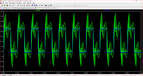
Sine wave 1kHz with multiple capacitance loads overlaid plot.
.asc file also. Higher Iq bias option.
Figures for individual capacitor loads - .step param CV list 5nF 10nF 100nF 220nF 470nF 1uF 2uF
0.004522%
0.004523%
0.004527%
0.004532%
.asc file also. Higher Iq bias option.
Figures for individual capacitor loads - .step param CV list 5nF 10nF 100nF 220nF 470nF 1uF 2uF
0.004522%
0.004523%
0.004527%
0.004532%
Last edited:
Sine wave 1kHz with multiple capacitance loads overlaid plot.
.asc file also. Higher Iq bias option.
Figures for individual capacitor loads - .step param CV list 5nF 10nF 100nF 220nF 470nF 1uF 2uF
0.004522%
0.004523%
0.004527%
0.004532%
Attachments
- Home
- Amplifiers
- Solid State
- One of the Top Solid-State CFA amp design