I have been looking at square wave testing. The dc offset in the attached .asc file is +14 mV. The circuit does require an output coil to be stable.
This is SE, no balanced input?
Perhaps we need to connect signal source like this? But cold input isn't a return for hot input. Than there should be return from differential signal source?
Maybe that version distorts if the signal to the cold input is in opposite phase to the hot input because of absence of return?
Attachments
This is SE, no balanced input?
Perhaps we need to connect signal source like this? But cold input isn't a return for hot input. Than there should be return from differential signal source?
Maybe that version distorts if the signal to the cold input is in opposite phase to the hot input because of absence of return?
It is clear from my simulations that this circuit performs better when the hot and cold input signals are in the same phase. The reasons for the deficiency with opposite phase were given by keantoken in post 182 on page 19 - re impacts on the nfb due to R2 and R4 forming an alternative decoupling route to earth.
This increases the closed loop gain significantly and reduces the feedback factor a situation that does not arise with identical input phase signals on hot and cold.
With signals on hot and cold inputs with the same voltage but opposite in phase the THD is about 2%.
Looking at the circuit from a different viewpoint - in the positive rail half R2, R3, and R17 all share a common supply rail with Q1 and Q12 sharing the same configuration.
In the case of identical phase input signals on the hot and cold terminals an increase in a negative going signal will cause Q1 and Q12 to draw more current.
On the opposite side of the circuit this will cause Q2 and Q13 to draw less current. The cycle reverses when the input signal goes negative.
Importantly the current flow through all these transistors does not cut off in their push pull action.
When the signal inputs to hot and cold are in opposite phase the action becomes partial push-pull with zones where the above transistors will work in opposition to the point of becoming cut off.
This has been illustrated before in some of my earlier posts - you can refresh some of these images in SPICE to see this again.
I have looked at a method to change the circuit so it will operate with balanced inputs - but the simulation says THD is 0.3% which is senseless in view of the performance indicated with the same phase signals on hot and cold inputs. The figure 0.3% raises the question how stable is it?
At some point one has to call a halt in doing simulations - I have to return to my care obligations so I will be taking a break from DIY for a while.
In the meantime good luck with your endeavours.
Maybe someone on this forum will find the solution to use balanced inputs with decent THD.
In case of SE, this one should perform better.
Many thanks Mjona for your help and support. Take care of your wife.
Best Regards.
In case of SE, this one should perform better.
Many thanks Mjona for your help and support. Take care of your wife.
Best Regards.
Attachments
Last edited:
Maybe someone on this forum will find the solution to use balanced inputs with decent THD.
In case of SE, this one should perform better.
Many thanks Mjona for your help and support. Take care of your wife.
Best Regards.
Yes I will be doing that for six weeks - unfortunately your simulation does not have a load at the output - with 8R in place it is unstable.
I have gone back to the original circuit to see why you had problems with the dc offset adjustment knowing also that a lot of the circuit has been assumed to be correct.
The values for R10 and R11 were 2.2k in the version of the circuit running 60 volt rails in association with these. A value of 750R was substituted for 45 volt rails.
That does not help the coarse adjustment of 100R trim pot pairs to accuracy of an Ohm or less. If the resistance of either is set too high there will be a kink in the form of a sine wave.
It is possible this finicky business is responsible for what you were seeing on your 'scope .
In fact the circuit will work whichever way those CCS transistors are oriented on the pcb - I have done some further simulations - now attached.
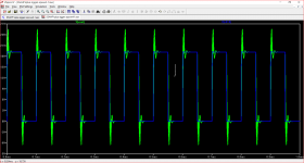
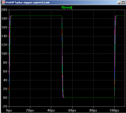
One of these is a 10 kHz square wave test with the merged section in the nfb line with a step response capacitor in parallel. In this alternative there is no overshoot in the wave before the output coil.
The ripples after the coil represent the selection of capacitors from 10n to 2uF in one shot.
With the original network as used in the 1kHz sine wave test simulation - there is a single overshoot which many would overlook - but overall the amplifier should be stable with reactive loads and it will be convenient not to alter your pcb.
I cannot give you any good news about achieving balanced operation.
I see some place in the original authors commentary mention of bridging stereo pairs to increase power output?
Anyway, if the dc adjustment is correctly set the original configuration has the lower THD result.
I have changed the emitter resistor values to those given by Lazy Cat and set the current to give close to 27 mV across these.
Attachments
It's stable with 8R load if to increase Cdom caps on drivers to 150pF. However the most important to know why the schematic require so big cdom to be stable? I think in SE config we can remove small VAS transistors, maybe it will become more stable with lower value compensation.
DC offset I had before was because of different characteristics of NPN PNP transistors causing asymmetry in operation. That's why values on R8 R9 are not equal.
2.2K for R10 R11 was a mistake i think. If to check other designer's schematic, as well as other people similar ssa projects, these current set resistors were different values (1-1.5K for SE) which should provide enough current for ssa bridge to maintain stable 15V potential on zeners.
With these pots I can set the DC offset within 1-5mV range easily.
I also tried to simulate it with different ccs orientation, the best opt thd-wise for SE use like the original orientation.
What do you mean by "I see some place in the original authors commentary mention of bridging stereo pairs to increase power output?" I don't need bridging or increase power output. 3 output pairs should provide plenty of power I guess.
Last edited:
I have omitted R39 R40 (2R2) as they are not required. thd is unbelievable.
Attachments

Last edited:
It's stable with 8R load if to increase Cdom caps on drivers to 150pF. However the most important to know why the schematic require so big cdom to be stable? I think in SE config we can remove small VAS transistors, maybe it will become more stable with lower value compensation.
DC offset I had before was because of different characteristics of NPN PNP transistors causing asymmetry in operation. That's why values on R8 R9 are not equal.
2.2K for R10 R11 was a mistake i think. If to check other designer's schematic, as well as other people similar ssa projects, these current set resistors were different values (1-1.5K for SE) which should provide enough current for ssa bridge to maintain stable 15V potential on zeners.
With these pots I can set the DC offset within 1-5mV range easily.
I also tried to simulate it with different ccs orientation, the best opt thd-wise for SE use like the original orientation.
What do you mean by "I see some place in the original authors commentary mention of bridging stereo pairs to increase power output?"
This simulation is of the earlier circuit which does not purport to be balanced so the last question is not relevant.
More to the point there is a problem with the output stage current consumption in this.
Some small changes in this circuit can have a disproportionate affect on performance results.
For instance a small change could upset the dc offset, or increase the THD, or reduce the circuit stability.
Anyway I have done a pair of simulations one of THD and one of square wave performance.
By this means I was able to cross check the results on two fronts by making the same change in each simulation - taking things one step at a time.
I have checked the square wave simulation with a variety of capacitors in parallel with 8R with varying signal input levels monitoring the result at node n20 - I have seen circuit simulations where a malfunction occurs at a low level input signal level.
I don't have the time to fine tune at length - the dc offset is 22 mV
The file is attached for reference purposes.
Attachments
Do you know why there are problems with the output stage current consumption and the disproportionate affect on performance results? Is this due to phase margin (nyquist stability) related?More to the point there is a problem with the output stage current consumption in this.
Some small changes in this circuit can have a disproportionate affect on performance results.
For instance a small change could upset the dc offset, or increase the THD, or reduce the circuit stability.
Anyway I have done a pair of simulations one of THD and one of square wave performance.
By this means I was able to cross check the results on two fronts by making the same change in each simulation - taking things one step at a time.
I have checked the square wave simulation with a variety of capacitors in parallel with 8R with varying signal input levels monitoring the result at node n20 - I have seen circuit simulations where a malfunction occurs at a low level input signal level.
.
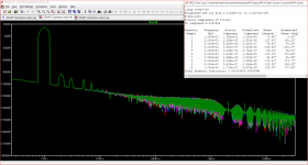
In my simulation THD depends on input capacitor used. 100uF isn't a practical value. I would use 1-4uF in that place.
Your last asc file don't show THD and FFT simulation in usual way. Maybe I doing something wrong.
As I see, you changed input bias cuurent much and Vbe multiplier circuit. Recommended input bias current 3-4mA per device. I've never seen such a high Vbe multiplier resistance. Is this bacause of raised input bias current?
Why have you changed R21 and drivers bias current?
What malfunction do you mean at low level input signal?
Do you know why there are problems with the output stage current consumption and the disproportionate affect on performance results? Is this due to phase margin (nyquist stability) related?
In my simulation THD depends on input capacitor used. 100uF isn't a practical value. I would use 1-4uF in that place.
Your last asc file don't show THD and FFT simulation in usual way. Maybe I doing something wrong.
As I see, you changed input bias cuurent much and Vbe multiplier circuit. Recommended input bias current 3-4mA per device. I've never seen such a high Vbe multiplier resistance. Is this bacause of raised input bias current?
Why have you changed R21 and drivers bias current?
What malfunction do you mean at low level input signal?
I have sent you a private message.
Stable ver. on lower currents
There are two changes that will make your amplifier stable.
First change your VAS transistor connections so C34 connects between the collector of Q16 and likewise so the base of Q14 and C36 connects between the collector of Q17 and the base of Q18.
Second you need an output coil 10uH //10R looks tidier in simulations of square waves but you might get away with 2uH.
C3 at the input does not affect the simulations - it appears to be superfluous.
The amplifier is running heavily into Class A with an output standing current of 900 mA.
If you reduce this operating level you will need to repeat your simulation tests as operating in this mode has mitigating effects on circuits.
I have attached the square wave simulation so you can cross check the results of any changes in your sine wave simulation.
Attachments
First change your VAS transistor connections so C34 connects between the collector of Q16 and likewise so the base of Q14 and C36 connects between the collector of Q17 and the base of Q18.
Second you need an output coil 10uH //10R looks tidier in simulations of square waves but you might get away with 2uH.
The amplifier is running heavily into Class A with an output standing current of 900 mA.
If you reduce this operating level you will need to repeat your simulation tests as operating in this mode has mitigating effects on circuits.
What do you mean by "the base of Q14 and C36 connects between the collector of Q17 and the base of Q18"?
It's stable even at 176 mA and with 1uH, 100p compensation caps.
Output coil destroys HF response. Does it possible to omit it somehow? Maybe short speaker cables needed?
Attachments
Last edited:
What do you mean by "the base of Q14 and C36 connects between the collector of Q17 and the base of Q18"?
It's stable even at 176 mA and with 1uH, 100p compensation caps.
Output coil destroys HF response. Does it possible to omit it somehow? Maybe short speaker cables needed?
You have interpreted the meaning correctly looking at your revised simulation - "Q14" should have preceded the words "likewise so" in my explanation.
As I have pointed out at length square wave testing looks at what is going on in the MHz response region which is a great step up above 10kHz.
If you look at the square wave plot at node 18 you will see the shape is still square - this shown in blue in the attachment.
You will always have an element of inductance in speaker cable and capacitance as well - so these can be reactive enough to cause oscillation - as a friend of mine found out when he used some performance cable with his new amplifier - which was affected so badly that it caused the transformer to fail.
Naim Audio have a cable manufactured to their requirements to suit their amplifiers. Instead of an output coil they substitute a 0.22 R resistor as an output buffer. Possibly with the right length of this cable and the resistor you might have a good result - this would be a matter of getting the right inductance in the cable which is quite expensive stuff.
Using another brand cable voids their warranty.
The best you can do is to use a coil with a value that suits your set-up including the speaker cables.
Attachments
reduced loop gain in the complementary triples
Add degeneration resistors to Q18 and Q19 as mentioned by john_ellis and Douglas Self. Circuit attached.
The output inductor can be left out if a 0.2 ohm 5W wire wound resistor is used instead. And if a troublesome cable cause oscillation then add another 0.2 ohm at the output terminal. See plot with 0.2 ohms -- no ringing with no inductor.
I haven't optimized R18, R22, R37 combination (and lower half R's). There may be slightly better values.
Attachments


Add degeneration resistors to Q18 and Q19 as mentioned by john_ellis and Douglas Self. Circuit attached.
The output inductor can be left out if a 0.2 ohm 5W wire wound resistor is used instead. And if a troublesome cable cause oscillation then add another 0.2 ohm at the output terminal. See plot with 0.2 ohms -- no ringing with no inductor.
I haven't optimized R18, R22, R37 combination (and lower half R's). There may be slightly better values.
Could you please advise how to optimize them? What values can be better?
Last edited:
Add degeneration resistors to Q18 and Q19 as mentioned by john_ellis and Douglas Self. Circuit attached.
The output inductor can be left out if a 0.2 ohm 5W wire wound resistor is used instead. And if a troublesome cable cause oscillation then add another 0.2 ohm at the output terminal. See plot with 0.2 ohms -- no ringing with no inductor.
I haven't optimized R18, R22, R37 combination (and lower half R's). There may be slightly better values.
There seems to be a problem with this on 1kHz sine input when asked to output c. 60 volts peak to peak in my simulation I get THD of 1%.
I think R18 should be a lot lower in value - in the order of a few Ohms.
I have changed two resistor values in each driver half of the attached simulation - at 1kHz contrary to the file title. THD is reduced to 0.00026%.
I have not checked at 20k sine or square wave.
Attachments
Optimizing degeneration of the output triple
Optimizing R18 (=R36) degeneration of the triple worked best for me. Adding a resistor in the emitter of the first transistor "NPN" didn't help in this case (although other times it has helped me).
Changing R18 (=R36) also changes the idle current so R37(=R38) and R22 (=R23) need to change to get back to the original idle current (which was 308mA is the circuit prior to y post).
I originally started with R22 (=R23) of 330 ohms rather than the original 150 ohms and then changed R37 (=R38) to get the original 300mA idle current, that's after trying different R18 (=R36) values until I damped out
oscillation (and most of the ringing) while using a small value of R17 (the output series resistor in place of the L//R network). Then I stepped CV load capacitor to see which values caused the most ringing.
A recommended approach:
After discovering the worst ringing is with CV fixed at 100nF and R22 & R23 can be fixed 150 ohms as original.
Also R17 (output R) can be set at 1m (effectively zero). Monitor Vfb output prior to R17.
We have now reduced the number of variables to one for no ringing, being R18 & R36. See below R18 & R36 stepped 22, 33, 47 ohms. Ringing with 22R. 47R chosen.
Once the ringing is stopped then R37 & R38 are trimmed for idle current. 120 ohms used.
Then add R17. EG check 0.1 ohms with all CV range.
Bench tests are needed to finalize values for R18 & R36 due to neglected model and board wiring effects. It may require twice the simulated minimum value for R17 and or slight increase in R18 & R36 etc.
----------
Epilogue: After optimizing the clip recovery was checked. It was noticed that there was a low level HF oscillation that started in the -25V to -15V output voltage range. Note the positive side does not oscillate, only the negative half of the output waveform in a certain voltage range. First I tried changing R18 & R36 degeneration as above for both sides did not stop this oscillation, nor did changing R36 only for the negative side.
This oscillation was stopped by increasing the base stopper resistors R27,R28,R29 on the negative side.
Plots and sim circuits for the negative side problem are in a following post.
Could you please advise how to optimize them? What values can be better?
Optimizing R18 (=R36) degeneration of the triple worked best for me. Adding a resistor in the emitter of the first transistor "NPN" didn't help in this case (although other times it has helped me).
Changing R18 (=R36) also changes the idle current so R37(=R38) and R22 (=R23) need to change to get back to the original idle current (which was 308mA is the circuit prior to y post).
I originally started with R22 (=R23) of 330 ohms rather than the original 150 ohms and then changed R37 (=R38) to get the original 300mA idle current, that's after trying different R18 (=R36) values until I damped out
oscillation (and most of the ringing) while using a small value of R17 (the output series resistor in place of the L//R network). Then I stepped CV load capacitor to see which values caused the most ringing.
A recommended approach:
After discovering the worst ringing is with CV fixed at 100nF and R22 & R23 can be fixed 150 ohms as original.
Also R17 (output R) can be set at 1m (effectively zero). Monitor Vfb output prior to R17.
We have now reduced the number of variables to one for no ringing, being R18 & R36. See below R18 & R36 stepped 22, 33, 47 ohms. Ringing with 22R. 47R chosen.
Once the ringing is stopped then R37 & R38 are trimmed for idle current. 120 ohms used.
Then add R17. EG check 0.1 ohms with all CV range.
Bench tests are needed to finalize values for R18 & R36 due to neglected model and board wiring effects. It may require twice the simulated minimum value for R17 and or slight increase in R18 & R36 etc.
----------
Epilogue: After optimizing the clip recovery was checked. It was noticed that there was a low level HF oscillation that started in the -25V to -15V output voltage range. Note the positive side does not oscillate, only the negative half of the output waveform in a certain voltage range. First I tried changing R18 & R36 degeneration as above for both sides did not stop this oscillation, nor did changing R36 only for the negative side.
This oscillation was stopped by increasing the base stopper resistors R27,R28,R29 on the negative side.
Plots and sim circuits for the negative side problem are in a following post.
Attachments

Optimizing negative side base stopper resistors to stop HF osc
As mentioned in the post above on optimizing the degeneration resistors for the triples I checked clip recovery.
It was noticed that there was a low level HF oscillation that started in the -25V to -15V output voltage range. Note the positive side does not oscillate, only the negative half of the output waveform in a certain voltage range.
I first tried changing R18 & R36 degeneration as above for both sides but this did not stop this oscillation, nor did changing R36 only for the negative side.
This oscillation was stopped by increasing the base stopper resistors R27,R28,R29 on the negative side.
Base resistors R27,R28,R29 were increased to 5R6 (originally 2R2 like the upper half).
Also, to keep R27,R28,R29 to a minimum the value of resistor R42 (in series with C20) was increased to 5R6 (originally 0.8 ohms). This stopped the oscillations on the negative side for all output voltages and CV values.
BTW capacitor C20 couples the bases of the power transistors and increasing R42 in series with C20 seems to decouple a troublesome and unexpected HF circulation path between the upper and lower transistors.
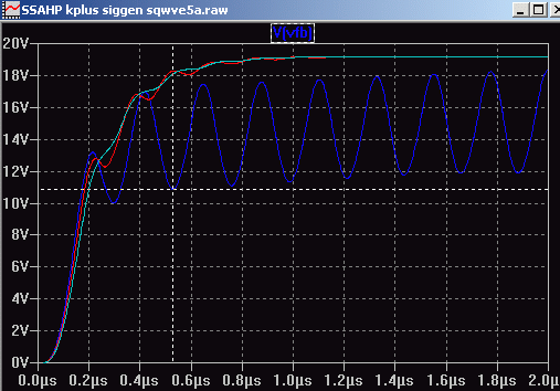
A plot with a 3Vpk 20kHz sinewave clipping shows clip recovery is clear of ringing. Nice.

However, a weak HF oscillation between -25V and -15V (last part of sinewave) can be seen in a zoom below. Here the base resistors are stepped on the negative side only from 5R6 to 2R2 (original value)

The oscillation is with 2R2 base resistors (blue) and no oscillation with 5R6 (green). Other values used are R18=47R, R19=150R, R37=120R, R17=0.22, and upper base stoppers are still 2R2. The sim file is supplied.
How to optimize R42:
First optimze the degeneration resistors (as covered in the other post) to get one side free of oscillation for any CV loading with the output series resistor.
Use a simewave that clips so you can cover the full output range.
Step Rb for the the negative side base resistors working backwards eg 6R8 5R6 4R7 3R3 2R2. Watch which step causes the simulation to crawl when it breaks into oscillation. Stop the simulation and increase R42 eg 0.8R originally to say 10 ohms.
ReRun. If all the steps are clear of oscillation reduce R42.
If it oscillates at one of the steps then try a higher value of R42 until there is no change in the step it oscillates -- so choose a the value of R42 one or two steps higher than the one it oscillates at.
Fix Rx at this value (disable the Step command for Rx).
Reduce R42 until oscillation starts again and then use say double that minimum value. I found R42 could be 5R6 and Rb (R27,R28,R29) is also 5R6 (coincidence?)
...Plots and sim circuits for the negative side problem are in a following post.
As mentioned in the post above on optimizing the degeneration resistors for the triples I checked clip recovery.
It was noticed that there was a low level HF oscillation that started in the -25V to -15V output voltage range. Note the positive side does not oscillate, only the negative half of the output waveform in a certain voltage range.
I first tried changing R18 & R36 degeneration as above for both sides but this did not stop this oscillation, nor did changing R36 only for the negative side.
This oscillation was stopped by increasing the base stopper resistors R27,R28,R29 on the negative side.
Base resistors R27,R28,R29 were increased to 5R6 (originally 2R2 like the upper half).
Also, to keep R27,R28,R29 to a minimum the value of resistor R42 (in series with C20) was increased to 5R6 (originally 0.8 ohms). This stopped the oscillations on the negative side for all output voltages and CV values.
BTW capacitor C20 couples the bases of the power transistors and increasing R42 in series with C20 seems to decouple a troublesome and unexpected HF circulation path between the upper and lower transistors.
A plot with a 3Vpk 20kHz sinewave clipping shows clip recovery is clear of ringing. Nice.
However, a weak HF oscillation between -25V and -15V (last part of sinewave) can be seen in a zoom below. Here the base resistors are stepped on the negative side only from 5R6 to 2R2 (original value)
The oscillation is with 2R2 base resistors (blue) and no oscillation with 5R6 (green). Other values used are R18=47R, R19=150R, R37=120R, R17=0.22, and upper base stoppers are still 2R2. The sim file is supplied.
How to optimize R42:
First optimze the degeneration resistors (as covered in the other post) to get one side free of oscillation for any CV loading with the output series resistor.
Use a simewave that clips so you can cover the full output range.
Step Rb for the the negative side base resistors working backwards eg 6R8 5R6 4R7 3R3 2R2. Watch which step causes the simulation to crawl when it breaks into oscillation. Stop the simulation and increase R42 eg 0.8R originally to say 10 ohms.
ReRun. If all the steps are clear of oscillation reduce R42.
If it oscillates at one of the steps then try a higher value of R42 until there is no change in the step it oscillates -- so choose a the value of R42 one or two steps higher than the one it oscillates at.
Fix Rx at this value (disable the Step command for Rx).
Reduce R42 until oscillation starts again and then use say double that minimum value. I found R42 could be 5R6 and Rb (R27,R28,R29) is also 5R6 (coincidence?)
Oops
Yes, I got the same 1% with my (high) degeneration value and with my base stopper mods as well.
But with your mods it does oscillate at 20kHz.
So I tried my base stopper mods and my C20's series R42 with your degeneration resistor of 2.2 ohms etc and it now works good -- no oscillation with 20kHz and low 0.00026% distortion at 1kHz 60Vpp 🙂.
So my post on optimizing the degeneration resistor must have given a local optimum and not the the global optimum. 😱
Rather than step 22 ohms and above it needs to step from an ohm and above. But what prevented me from doing this was another oscillation coming from the negative half, which it seems, needed to be cured first before the degeneration could be optimized.
So team work has done it, but not in a linear way.
Thanks mjona!

Yes, it seems my optimum is not a good one for low distortion.There seems to be a problem with this on 1kHz sine input when asked to output c. 60 volts peak to peak in my simulation I get THD of 1%.
I think R18 should be a lot lower in value - in the order of a few Ohms.
I have changed two resistor values in each driver half of the attached simulation - at 1kHz contrary to the file title. THD is reduced to 0.00026%.
I have not checked at 20k sine or square wave.
Yes, I got the same 1% with my (high) degeneration value and with my base stopper mods as well.
But with your mods it does oscillate at 20kHz.
So I tried my base stopper mods and my C20's series R42 with your degeneration resistor of 2.2 ohms etc and it now works good -- no oscillation with 20kHz and low 0.00026% distortion at 1kHz 60Vpp 🙂.
So my post on optimizing the degeneration resistor must have given a local optimum and not the the global optimum. 😱
Rather than step 22 ohms and above it needs to step from an ohm and above. But what prevented me from doing this was another oscillation coming from the negative half, which it seems, needed to be cured first before the degeneration could be optimized.
So team work has done it, but not in a linear way.
Thanks mjona!
Attachments
- Home
- Amplifiers
- Solid State
- One of the Top Solid-State CFA amp design