One way to look at C20 is to compare it to the combined Cbe of the output transistors. If each transistor has say 10nF Cbe, then the total base load capacitance at the driver emitters would be 60nF. This is the capacitance C20 is intended to help drive, so it is apparent that C20>>Cbtotal. A factor of 5 would be fine. This results in a 300nF capacitor.
If you use more than this then you are compensating for something other than the BJT capacitive base drive signals. It comes down to an attempt to smooth the bias voltage. The problem is that it only partly works, and tends to even have the effect of worsening dynamic bias stability.
I brought this problem up earlier in a longer post here:
http://www.diyaudio.com/forums/soli...ab-power-amp-200w8r-400w4r-6.html#post3502255
Last edited:
One way to look at C20 is to compare it to the combined Cbe of the output transistors. If each transistor has say 10nF Cbe, then the total base load capacitance at the driver emitters would be 60nF. This is the capacitance C20 is intended to help drive, so it is apparent that C20>>Cbtotal. A factor of 5 would be fine. This results in a 300nF capacitor
Don't you mean output capacitance or Cob of output transistors? They have 145pF and 240pF each.
I just copied the values of C20/R42 from other schematic, I thought it was for hf filtering. Please feel free to change any component think right.
Several posts ago, AndriyOL raised a point about the level of current in the front end of an earlier simulation using the component values that have been carried over into your latest version.
You set bias current to 6.5mA/6mA of LTP transistors. As I know recommended current is 3-4.5mA, as increasing this value you also increase a GBW of the system, perhaps phase margin and the risk of oscillation. This will require the change of Vbe multiplier values.
Last edited:
Have you tried to use caps or CR combination to remove oscillation in that place?I also added further degeneration for the CFP driver, now in the emitter of the first and the base of the second transistor. The emitter degeneration of the second transistor has been discarded because the new combination seems to be better.
Without the emitter degeneration in the first transistor there was an oscillation at 1kHz but did not show any of the other tests, hence the need for this latest approach.
With this further degeneration for the CFP driver I returned to the original base resistors or 2R2 and 0.1 ohm emitter resistors and all seems to be well.
This latest combination is now stable at 1kHz and 20kHz sine, also with the fast rise squarewave and the full range of CV (Cout), and 50nH emitter resistors and 0.2 ohm +50nH output resistor. Sims are files attached. Idle current is reset to 300mA and distortion is 0.00035% at 1kHz and .
As Johnego said in post 150, 'base stopper has little effect unless you use high value resistor (it is usually used for trimming only). Capacitor is the main tool for compensation'.
I was thinking of RC combination at the driver base on negative side as was in original schematic.
The output emitter resistors I'm using have <5nH. They are cheap, small and affordable. Why we have to use inferior parts? Or you set this value for wirewound resistors to omit output inductor?
We can try to use higher voltage rails to increase stability, like 50/40V. I remember the stability was better in simulation if I set the same voltage for front end and output of the amp. Perhaps ideally the gap should be not less than 5V between two parts.
Last edited:
You set bias current to 6.5mA/6mA of LTP transistors. As I know recommended current is 3-4.5mA, as increasing this value you also increase a GBW of the system, perhaps phase margin and the risk of oscillation. This will require the change of Vbe multiplier values.
You will be pleased to know with the change in values mentioned in my previous post the current in the input cross LTP pairs is reduced to be in the order of 3.45 mA
Cbe is the capacitance of the base-emitter junction. For output transistors it is usually very large compared to Cob.
Why it's not mentioned in datasheet, only Cob?Cbe is the capacitance of the base-emitter junction. For output transistors it is usually very large compared to Cob.
There are many parameters not mentioned in the datasheet, Cbe belongs to the set of data they leave out because to most customers it isn't critical.
One way to look at C20 is to compare it to the combined Cbe of the output transistors. If each transistor has say 10nF Cbe, then the total base load capacitance at the driver emitters would be 60nF. This is the capacitance C20 is intended to help drive, so it is apparent that C20>>Cbtotal. A factor of 5 would be fine. This results in a 300nF capacitor.
If you use more than this then you are compensating for something other than the BJT capacitive base drive signals. It comes down to an attempt to smooth the bias voltage. The problem is that it only partly works, and tends to even have the effect of worsening dynamic bias stability.
I brought this problem up earlier in a longer post here:
http://www.diyaudio.com/forums/soli...ab-power-amp-200w8r-400w4r-6.html#post3502255
This picture shows there is a rift in the current wave form through C20
Attachments

You will be pleased to know with the change in values mentioned in my previous post the current in the input cross LTP pairs is reduced to be in the order of 3.45 mA
I wrote this because after this change the whole compensation and schematic could be different than current one we are exploring. However I'm not sure if such higher bias current values is better or not compared to usual 3-4mA. Higher GBW isn't bad, it provides wider frequency responce, if it can be handled right. Perhaps there should be some sweet spot like with output bias current for minimal crossover distortion.
That looks like one of the transistors is hitting saturation, plot the base current of each transistor to see if there is a bump in the waveform at the crest.
That looks like one of the transistors is hitting saturation, plot the base current of each transistor to see if there is a bump in the waveform at the crest.
That is Ian Hegglun's simulation - Australia where he lives the time is a few hours behind New Zealand on the clock.
I have my own to look into further in the morning - I am seeing a sawtooth pattern for the current through C20.
A sawtooth pattern is normal for this cap when operating in full class AB at medium or high power.
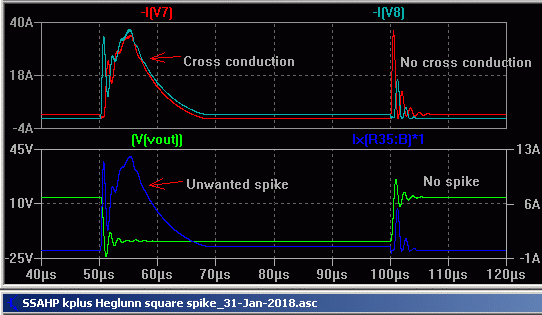
Hi mjona, keantoken,
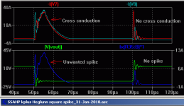
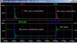
Attached is the circuit set so it generates a cross-conduction spike.

Settings are R44/R46 2R, Ls 100n, R37/R38 30R (for near original idle current).
The rising edge (right 100us) does not have any cross-conduction.
The falling edge (left 50us) has nearly 40A of cross-conduction at the peak.
Next break R42/C20 link and re-run with all other values the same, gives no cross conduction spike
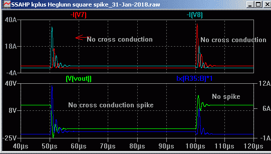
showing it is current through R42/C20 that can cause this unwanted cross-conduction under certain conditions.
Attached is the circuit set so it generates a cross-conduction spike.
Settings are R44/R46 2R, Ls 100n, R37/R38 30R (for near original idle current).
The rising edge (right 100us) does not have any cross-conduction.
The falling edge (left 50us) has nearly 40A of cross-conduction at the peak.
Next break R42/C20 link and re-run with all other values the same, gives no cross conduction spike
showing it is current through R42/C20 that can cause this unwanted cross-conduction under certain conditions.
Attachments
Why a CFP triple needs degeneration resistors and not caps
In a simulation you should step the inductance to find how high it can go before it loses stability and then design for half that value so you have a 'safety factor' -- which often gets swallowed up by unaccounted for inductances or random variations in parts.
I agree a 'Capacitor is the main tool for compensation' -- in your circuit C34,C35 (100pF) provide the primary compensation to obtain the gain and phase margin which can be done using the 'AC' simulation.
However, there can be hidden instabilities due to Class-AB switching effects, as in this case in the CFP driver. This is because the AC run only plots at the idle current operating point and doesn't consider changes in gain and capacitances and FT over the whole operating current and voltage range.
This is the cause of the difficulty. So we need to make the CFP driver less nonlinear and this is best done with degeneration resistor in the emitter of the first transistor and another in the second complementary transistor (Q18,Q19).
BTW the CFP is usually inherently stable when operated in Class-A; it's a winner in Class-A as Douglas Self showed many years ago in his book. This is because in Class-A the transistors don't turn off. Unfortunately, I don't know of a simple way to modify this type of output stage to keep the CFP driver transistors conducting slightly when one side turns off in Class-AB. The FT of the CFP and the power transistors plummet when they turn off in Class-AB which means extra compensation and extra degeneration is needed to stabilize this CFP triple output stage over the full range of CV loads, currents and voltages.
The value of 50nH that I was using for my simulation shows that it can be made stable even with relatively high inductances. Bear in mind there is 20nH per inch of interconnections including the power transistor emitter lead and bond wires and then to the output summing node....The output emitter resistors I'm using have <5nH. They are cheap, small and affordable. Why we have to use inferior parts? Or you set this value for wirewound resistors to omit output inductor?
In a simulation you should step the inductance to find how high it can go before it loses stability and then design for half that value so you have a 'safety factor' -- which often gets swallowed up by unaccounted for inductances or random variations in parts.
I don't know what the "RC combination at the driver base on negative side as was in original schematic" is so I can't comment on this....Have you tried to use caps or CR combination to remove oscillation in that place?
As Johnego said in post 150, 'base stopper has little effect unless you use high value resistor (it is usually used for trimming only). Capacitor is the main tool for compensation'.
I was thinking of RC combination at the driver base on negative side as was in original schematic.
I agree a 'Capacitor is the main tool for compensation' -- in your circuit C34,C35 (100pF) provide the primary compensation to obtain the gain and phase margin which can be done using the 'AC' simulation.
However, there can be hidden instabilities due to Class-AB switching effects, as in this case in the CFP driver. This is because the AC run only plots at the idle current operating point and doesn't consider changes in gain and capacitances and FT over the whole operating current and voltage range.
This is the cause of the difficulty. So we need to make the CFP driver less nonlinear and this is best done with degeneration resistor in the emitter of the first transistor and another in the second complementary transistor (Q18,Q19).
BTW the CFP is usually inherently stable when operated in Class-A; it's a winner in Class-A as Douglas Self showed many years ago in his book. This is because in Class-A the transistors don't turn off. Unfortunately, I don't know of a simple way to modify this type of output stage to keep the CFP driver transistors conducting slightly when one side turns off in Class-AB. The FT of the CFP and the power transistors plummet when they turn off in Class-AB which means extra compensation and extra degeneration is needed to stabilize this CFP triple output stage over the full range of CV loads, currents and voltages.
Last edited:
Cbe is the capacitance of the base-emitter junction. For output transistors it is usually very large compared to Cob.
I think the Cbe you are referring to is the junction capacitance when the output transistor is off. The Cbe in the hybrid pi model is much higher when the transistor is turned on, due to its ft. In the hybrid pi model, C_pi = gm/(2pi * ft). gm is pretty high when the transistor is on. Of course, all of this is only a small-signal approximation.
Cheers,
Bob
I don't know what the "RC combination at the driver base on negative side as was in original schematic" is so I can't comment on this.
By RC I mean like it's used here 100R+220p.
Attachments
A sawtooth pattern is normal for this cap when operating in full class AB at medium or high power.
C20 is 1uF in my simulation at 1kHz the sawtooth current hardly registers 0.06 mA. The waveform transforms to a spike of 770 mA at 20kHz.
The sawtooth shape loses it's form if the value of the cap is increased - peakier higher in magnitude - not a good look.
The value can be reduced but I have kept it to 1uF due to the slightly better shape given with square wave tests. Perhaps a matter of smoothing over something that could be better optimized in my simulation.
By RC I mean like it's used here 100R+220p.
That is lag compensation - fine tuning the relative phase in the negative half of the circuit.
If you are still working on getting your hardware running leave those parts in.
I will look at this later when I have more time.
Last edited:
I would continue to work on, but I don't know how to do all of these in LTSpice. The only simple mode works for me is 1K sine wave test). There is also no any usefull video on Youtube how to simulate amplifier in LTSpice
Hi mjona, keantoken,
Attached is the circuit set so it generates a cross-conduction spike.
Settings are R44/R46 2R, Ls 100n, R37/R38 30R (for near original idle current).
The rising edge (right 100us) does not have any cross-conduction.
The falling edge (left 50us) has nearly 40A of cross-conduction at the peak.
Next break R42/C20 link and re-run with all other values the same, gives no cross conduction spike

showing it is current through R42/C20 that can cause this unwanted cross-conduction under certain conditions.
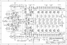
I notice some changes in the driver stage. For what it is worth I have seen stages like the original one on the thread - see attached.
I have looked on this as an exercise as developing a workable prototype so I have restricted my changes to component values with a couple of deletions.
I have noted the points made by Bob Cordell about circuit board layout so a re-work may be on the cards in which case the extra information may be relevant.
Attachments
- Home
- Amplifiers
- Solid State
- One of the Top Solid-State CFA amp design