Square wave tests of the circuit attached to my post 275 have shown a need to change some component values R37 and R38 reduce from 47R to 43R and R26 to R29 increase from 2R2 to 4R7.
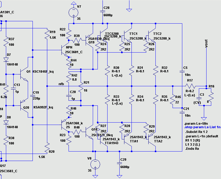
A perhaps unforeseen consequence of introducing the additional transistors Q18 and Q19 is these draw a substantial current through the cross coupling resistor R21 so these will need to be capable varying between 80 and 120 mA while dissipating 4W each.
For a 1.2V input the output into 8R plus the parallel test caps is close to 19 Volts peak regardless of the individual capacitor values.
The same input into the original form of the circuit indicates the voltage swing will be higher for the higher capacitor loads - e.g. 26 Volts peak in the case of 2uF.
The present circuit can match that if the signal input voltage is increased approaching 1.6 -1.7 V.
The output is dependent on the signal input and within whatever limitations the circuit has - not on the load.
Attachments
Yes, it seems my optimum is not a good one for low distortion.
Yes, I got the same 1% with my (high) degeneration value and with my base stopper mods as well.
But with your mods it does oscillate at 20kHz.
So I tried my base stopper mods and my C20's series R42 with your degeneration resistor of 2.2 ohms etc and it now works good -- no oscillation with 20kHz and low 0.00026% distortion at 1kHz 60Vpp 🙂.
So my post on optimizing the degeneration resistor must have given a local optimum and not the the global optimum. 😱
Rather than step 22 ohms and above it needs to step from an ohm and above. But what prevented me from doing this was another oscillation coming from the negative half, which it seems, needed to be cured first before the degeneration could be optimized.
So team work has done it, but not in a linear way.
Thanks mjona!

Something I'm not getting. With this sim THD is very good at 1KHz, but climbs sky high at 20KHz. Am I missing something?
Something I'm not getting. With this sim THD is very good at 1KHz, but climbs sky high at 20KHz. Am I missing something?
I made some changes to the circuit in post 275 and simulated with 20kHz, 1kHz sine inputs and 10 kHz square wave input - all into 8R with a range of test capacitance values in parallel.
Attachments
Harking back to page 5 - post 50 Douglas Self pointed out that triple output stages can be very hard to stabilise and he has avoided using them in his commercial designs.
He also mentions that parasitics can cause problems. With that in mind I modified the simulations in post 283 to reflect an element of parasitic inductance in wire-wound resistors which messes the simulations considerably.
There is a suitable Metal Film/Element type made by Bournes with 0.1R value - available from Digi-key - CRA2512-FZ-R100ELF with an inductance of <5nH. The output buffer resistor 0.22R should also be low inductance but it may require two 0.1R of the identified type - I have not been able to find an equivalent with 0.22R.
I think the circuit would stand a better chance of working with low inductance parts. I have changed the simulation for the buffer and emitter resistors but I doubt these would be the only parts needing to be re-specified.
Last edited:
So I tried my base stopper mods and my C20's series R42 with your degeneration resistor of 2.2 ohms etc and it now works good -- no oscillation with 20kHz and low 0.00026% distortion at 1kHz 60Vpp 🙂.
When I tried to change frequency to 20K on V3 voltage source the simulation isn't working right? Also changing back Rb to 2R2, removing R17 0R22 don't harm the simulation. Am I doing something wrong?
Is it possible to check frequency responce of this schematic?
What do you think about adding LC compensation to negative side, as was in original schematic, instead of raising Rb values to 5R6?
Last edited:
He also mentions that parasitics can cause problems. With that in mind I modified the simulations in post 283 to reflect an element of parasitic inductance in wire-wound resistors which messes the simulations considerably.
There is a suitable Metal Film/Element type made by Bournes with 0.1R value - available from Digi-key - CRA2512-FZ-R100ELF with an inductance of <5nH. The output buffer resistor 0.22R should also be low inductance but it may require two 0.1R of the identified type - I have not been able to find an equivalent with 0.22R.
I think the circuit would stand a better chance of working with low inductance parts. I have changed the simulation for the buffer and emitter resistors but I doubt these would be the only parts needing to be re-specified.
I'm using vishay wsh as emitter resistors in output stage. These are low inductance parts.
Is it possible to set inductance value for resistors in simulation?
Why have you chosen to run such a high input bias current of LTP transistors? I was aimed to almost twice a lower value.
Last edited:
Lately I've been working on a circuit with LTspice. When I added some more voltage and current gain, changing it from having two to having three voltage gain stages, I couldn't stabilize it just by trying different values of the phase compensation capacitor connected between the output stage and the input stage. I hadn't thought of trying adding some Cdom capacitance at the time. However, having only two voltage gain stages makes the amplifier design simpler. Also, with only two voltage gain stages, it was being stable even without the phase compensation capacitor.
Lately I've been working on a circuit with LTspice. When I added some more voltage and current gain, changing it from having two to having three voltage gain stages, I couldn't stabilize it just by trying different values of the phase compensation capacitor connected between the output stage and the input stage. I hadn't thought of trying adding some Cdom capacitance at the time. However, having only two voltage gain stages makes the amplifier design simpler. Also, with only two voltage gain stages, it was being stable even without the phase compensation capacitor.
Could you please share the sim file here?
Could you please share the sim file here?
It was frustrating when I shared one of my best ideas because it seemed to infringe on someone's patent. That took a lot of the fun out of the whole thing. I can give the request some more thought though. However, anyhow, I don't think I can take a critique of it.
It was frustrating when I shared one of my best ideas because it seemed to infringe on someone's patent. That took a lot of the fun out of the whole thing. I can give the request some more thought though. However, anyhow, I don't think I can take a critique of it.
More thought to the request would be much appreciated and for sure won't be any critique from my side.
Electrone, don't let one spoilsport affect your outlook for a whole category of undertakings. Knowing about the patent allows you to do more, not less, whereas unintentionally using a patented circuit can cause a lot of setbacks.
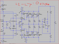
Subcircuit for inductive resitors
LTspice does not seem to allow 'Lser' parameter with a standard resistor so you have to use a subcircuit for now.
This requires a custom symbol I call "Rx.asy" (included in the zip file) and Rx subcircuit (already included on the circuit) which is:
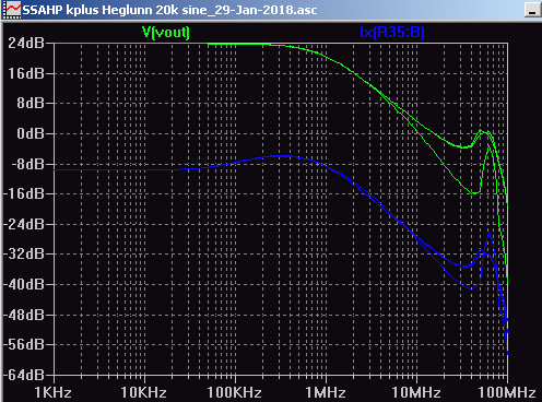
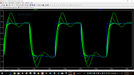
The plot shows the effect of emitter resistor series inductance on the AC response as I(R35) which affects the 10MHz-50MHz region (see below). All 6 emitter resistors have inductance stepped 0n 5nH 100nH. Also R17 is stepped (same values) so the effect of resistor series inductance for R17 can be seen in the V(vout) plot.
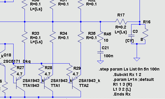
A tip for using this subcircuit is the Ls parameter can be defined as a fixed value and then hidden from view to avoid clutter. Right click on the resistor and set L=<myvalue> and to hide it double click the 'X' in the Vis column. You can tell which resistors are subcircuits because the use "R=0.2".
Another tip is when first placing the subcircuit resistor you change it from U1 to R<#> where # is the next available resistor number (which you find by adding a standard R then deleting it). After setting the first subcircuit resistor number then the next are automatic when you use F6 to copy the last one.
-------
Re: Post #284 mjona on obtaining low inductance resistors
Bob Cordell likes 2W or 3W metal film resistors because they are low inductance and low cost. To get to higher wattage parallel several (eg stack them to save PCB area). See the attached section from his book p201 (with permission).
BTW I don't see any need for a low inductance resistor for R17 (which replaces the output inductor) because it is outside the feedback loop.
The attached circuit has inductive emitter resistors as a subcircuit.I'm using vishay wsh as emitter resistors in output stage. These are low inductance parts.
Is it possible to set inductance value for resistors in simulation?
...
LTspice does not seem to allow 'Lser' parameter with a standard resistor so you have to use a subcircuit for now.
This requires a custom symbol I call "Rx.asy" (included in the zip file) and Rx subcircuit (already included on the circuit) which is:
.Subckt Rx 1 2
.param L=1n ;default
R1 1 3 {R}
L1 3 2 {L}
.Ends Rx
.param L=1n ;default
R1 1 3 {R}
L1 3 2 {L}
.Ends Rx
The plot shows the effect of emitter resistor series inductance on the AC response as I(R35) which affects the 10MHz-50MHz region (see below). All 6 emitter resistors have inductance stepped 0n 5nH 100nH. Also R17 is stepped (same values) so the effect of resistor series inductance for R17 can be seen in the V(vout) plot.
A tip for using this subcircuit is the Ls parameter can be defined as a fixed value and then hidden from view to avoid clutter. Right click on the resistor and set L=<myvalue> and to hide it double click the 'X' in the Vis column. You can tell which resistors are subcircuits because the use "R=0.2".
Another tip is when first placing the subcircuit resistor you change it from U1 to R<#> where # is the next available resistor number (which you find by adding a standard R then deleting it). After setting the first subcircuit resistor number then the next are automatic when you use F6 to copy the last one.
-------
Re: Post #284 mjona on obtaining low inductance resistors
Bob Cordell likes 2W or 3W metal film resistors because they are low inductance and low cost. To get to higher wattage parallel several (eg stack them to save PCB area). See the attached section from his book p201 (with permission).
BTW I don't see any need for a low inductance resistor for R17 (which replaces the output inductor) because it is outside the feedback loop.
Attachments
-
 SSAHP kplus Heglunn CCT step ind Re_29-Jan-2018.png7 KB · Views: 377
 -
SSAHP kplus Heglunn AC step Ls_29-Jan-2018.zip7.3 KB · Views: 87
-
RxSubcircuit.zip471 bytes · Views: 95
-
 SSAHP kplus Heglunn AC step ind Re_29-Jan-2018.png9 KB · Views: 367
 -
 Cordell-Power-Amp-Design-book-p201-1st-Ed.png44.9 KB · Views: 278
I notice a number of designs here using 0.1-ohm emitter resistors. I am not a big fan of such a low value, and in fact have never gone that low. That has been mainly for reasons of decreased thermal stability with such low values, particularly when multiple output pairs are in parallel. However, the concerns may go deeper than that, and in fact I wonder if the use of 0.1-ohm resistors is exacerbating stability problems in some of the examples here.
Here's why: There are intrinsic ohmic resistances within the output transistor, in the form of emitter resistance and base spreading resistance. Moreover, the base stopper resistors in the designs will add an ohmic component. If we have a 4.7-ohm base stopper and output transistor beta of 50, we see 0.1 ohm ohmic looking back into the emitter of the output transistor (even without parasitic resistances intrinsic to the transistor).
If we think about satisfying the Oliver criteria for minimal static crossover distortion, we realize that that 0.1 ohm looking into the emitter is effectively part of total Re. From the standpoint of the Oliver criterion, RE is now 0.2 ohm. And half of that resistance is poorly defined and subject to change with transistor operating point and frequency. It would seem we would certainly no longer bias the output stage with 26mV across the physical 0.1 Re.
Since that parasitic ohmic component is a function of frequency as a result of beta being a function of frequency, it has an inductive component. All of these "imperfections" are relative to the value of the physical Re employed. In a design with 2.2 ohm base stoppers and 0.22-ohm emitter resistors, the relative effect of these imperfections is 4 times smaller.
If we went with 0.1 emitter resistors with the best intentions of reducing static crossover distortion, and yet the 0.1 resistors make it more difficult to satisfy the Oliver criteria, have we done that in vain?
Just seems like some cause for pause.
Cheers,
Bob
I'm not a myth buster like Bob is, but during the period of silence look back at my posts 253,264, and 267
The attached circuit has inductive emitter resistors as a subcircuit.
<snip>
Thanks for this information. The only information I could find about inductance values in wire-wound resistors was a lot higher than those in the extract of Cordell's book.
The value of 70nH for an emitter value of 0.5 ohms matches closely to one of the values I considered previously in a simulation i.e. 0.47 ohms.
I took a short cut by replacing the emitter resistors in my simulation with inductors having a value of 0.47 ohms to see where this led.
As far as 10 kHz square wave testing is concerned the inductance limits the peak output somewhat which is not surprising since this involves a bandwidth reaching into the MHz domain.
I was not able to run this test on your latest simulation as an error message came up.
I explored the idea of replacing the output coil I had used with a buffer resistor of 220m allowing for some inductance.
While this buffer and the zobel network maybe outside the feedback loop these still connect to the inverting signal input via the route from the output via the feedback resistors.
My argument is inverting inputs are summing points. A portion of a signal fed back from a speaker will flow through the zobel network to earth - since this is an ac form the disturbance caused will generate a signal from earth back to the summing point.
Since inductance alters phase it is easy to set up an arrangement between these two signal arms which does not help stability.
If you would test your circuit with a 10kHz square wave signal with the settings PULSE(-0.9 0.9 0 100n 100n 50us 100us 8) see what your result is.
...I was not able to run this test on your latest simulation as an error message came up.
Yes, the problem is the line .step param Ls List 0n 5n 100n
Strange, Ls=0n is OK for AC runs but not .trans. A bug maybe?
Change it to
.step param Ls List 1n 5n 100n
...or better still .step param Ls List 1n 10n 50n
...If you would test your circuit with a 10kHz square wave signal with the settings PULSE(-0.9 0.9 0 100n 100n 50us 100us 8) see what your result is.
I tried that and noticed the massive current (2A peak) transient sent through the Zobel ground via R45 and C21. This is a serious practical concern to keep the induced voltages in the ground return of the Zobel out of sensitive parts of the amp. I ran into this problem with my BiModal PCB recently and used a separate track for the Zobel return to the power common.
A new change, that allows the Zobel to be reduced to say 22nF +22 ohms, is to add base stopper resistors to Q18 & Q19 and 100 ohms worked for me and allowed the Zobel to be reduced to 22nF+22 ohm Zobel --that's with 0.1 ohm+50nH emitter resistors, 4R7 power base stoppers -- using my sim with the subcircuit for inductive resistors.
With reduced Zobel values you can use a lower wattage Zobel resistor (Bob Cordell uses 2W or 3W MF) and ground loop current is reduced by a factor of 4.
With the base stoppers on Q18 & Q19 the distortion at 20kHz was about the same as without the stoppers and the idle current was about the same. So I hope base stoppers on Q18 & Q19 also work on your bench version.
These are good points. I often use 0.022uF and 10 ohms for the Zobel. A Capacitance of 0.1uF for the Zobel, as shown in that schematic, is unnecessarily high. I think 22 ohms in the Zobel is a little on the high side. The Zobel loop from where the output transistors connect to the output bus and to the place where the output transistors are bypassed to ground should be short. Proper Zobel operation at high frequencies is important, and inductance in this loop should be avoided. In the extreme, one can use a distributed Zobel network, with multiple smaller Zobels connected near the emitter circuit of each output pair.
I also like to have the P and N of each output pair be adjacent, rather than all of the P to one side and all of the N to the other side. The circulating currents of each P-N pair want to be resolved locally. Bear in mind that the sum of those currents will be sinusoidal, once resolved. To the extent possible, we also want those + and - rail currents resolved at the output stage on the board, rather then them be required to flow back to the power supply to be resolved. I always put at least 1000uF rail bypass right at the output stage. The grounds of these capacitors are connected together first, then routed with a single trace to the ground bus.
I also do not go out of my way to use heavy-AWG wire to connect the rail lines from the output board to the power supply. It is usually a short run and a tiny bit of resistance actually helps the resolution of the currents on the output board. Non-intuitive, I know. Those wires do get twisted together, and may also be twisted with the ground line back to the power supply. I have actually considered using star quad microphone cable for this short run.
I always connect the loudspeaker ground line at the output board ground bus, NOT back at the power supply. Not a star ground approach, I know. Blindly using a star ground architecture is not always a good idea. Always be mindful of where the ground currents are flowing, and take measures to make them flow where you want them to.
The layout in output stages is very important to achieving low distortion and good stability.
Cheers,
Bob
Thanks for sharing your knowledge - a lot to think about.
Your scheme for currents to flow to an output ground bus rather than star earth has reminded me of a project, having what I thought of as an attractive sound, that I built approaching 40 years ago.
I tried the scheme from that project in a simulation - albeit that my knowledge of SPICE is pretty basic, I have not gotten into including supply rail ripple etc.
From the results I had a tentative thought this scheme could be worth a look asking about to see if this has any merit or if this is heading off on a tangent.
In either case it won't matter to me since I will not be building this circuit.
Attachments
Thanks Bob. Mounting p- and n- pairs adjacent to each other in parallel output stages is the best way to avoid RF layout issues and I have used that on my latest amp PCB.
The latest simulation mods below with the Zobel capacitor split and feeding back into the rails rather than the power common. Good idea mjona.
I also added further degeneration for the CFP driver, now in the emitter of the first and the base of the second transistor. The emitter degeneration of the second transistor has been discarded because the new combination seems to be better.
Without the emitter degeneration in the first transistor there was an oscillation at 1kHz but did not show any of the other tests, hence the need for this latest approach.
With this further degeneration for the CFP driver I returned to the original base resistors or 2R2 and 0.1 ohm emitter resistors and all seems to be well.
This latest combination is now stable at 1kHz and 20kHz sine, also with the fast rise squarewave and the full range of CV (Cout), and 50nH emitter resistors and 0.2 ohm +50nH output resistor. Sims are files attached. Idle current is reset to 300mA and distortion is 0.00035% at 1kHz and 60Vpp.
Bob, you suggested my 22 ohm Zobel is a bit too large. I use a slightly larger value (in simulations and actual bench versions) than normal to first get it stable and compensate the amp, then I reduce the value to the normal 10 ohms (as two 22 ohms in parallel) as a safety factor .
I have reservations about R42+C20 across R21 -- it sometimes allows a cross conduction condition where the power transistor current spikes unnecessarily and may cause secondary breakdown failure if the amplifier oscillates in the 100kHz to MHz range. I simulated with R42 as specified (0.8 ohms) as well as 5R6 and open and did not see a lot of benefit using it. You could leave it in for now to see how it goes with the latest mods on the bench and if there is any HF oscillation then open R42 to check if this is the reason. You may risk losing a set of power transistors by leaving it in, but then you won't ever know if there is really a problem in practice with it or not. It's your call.
Attachments

Thanks Bob.
I have reservations about R42+C20 across R21 -- it sometimes allows a cross conduction condition where the power transistor current spikes unnecessarily and may cause secondary breakdown failure if the amplifier oscillates in the 100kHz to MHz range. I simulated with R42 as specified (0.8 ohms) as well as 5R6 and open and did not see a lot of benefit using it. You could leave it in for now to see how it goes with the latest mods on the bench and if there is any HF oscillation then open R42 to check if this is the reason. You may risk losing a set of power transistors by leaving it in, but then you won't ever know if there is really a problem in practice with it or not. It's your call.
Several posts ago, AndriyOL raised a point about the level of current in the front end of an earlier simulation using the component values that have been carried over into your latest version.
Consequently I increased the values of R8 and R 9 to 62.5 ohms and 60 ohms respectively - these values are responsible not only for the dc offset but also the current levels in Q16 and Q17 which will reduce to 8.5 mA with the changes - down from 45 mA.
This made a considerable difference in my simulation and suggest you try these values in yours.
- Home
- Amplifiers
- Solid State
- One of the Top Solid-State CFA amp design