That schematic is flawed. If the person who made it actually built the circuit, they would have found it didn't work right (assuming they bothered to test it).
The 1.5k and 100 ohm resistors are the feedback network. The problem is the second input pair shunts the 100 ohm resistors, so they become the effective feedback shunt resistance and the gain of the amp becomes much higher than it needs to be.
Whoever made this schematic expected to use two input pairs in parallel to create a negative input, but it doesn't work that way. If you check you will find it does not invert, it doesn't have the same gain as the first input, and it causes a lot of distortion even if on the surface it appears to work.
If you just desolder the second input pair you should have a circuit which in principal should perform well, but it won't have a negative input.
Last edited:
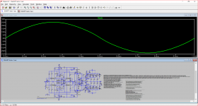
There is some confusion about the test method. I grounded the inverting input terminal having removed the "balanced" signal source to this and reduced the non inverting input signal to 0.3 V.
The attachment shows the result - just exactly how the actual hardware was tested is another question.
The attachment shows the result - just exactly how the actual hardware was tested is another question.
Attachments
So, there is no way to use differential input with this CFA schematic, very pity, only SE.
And a compensation of VAS and drivers can be tuned precisely with working simulation or maybe than it won't need the compensation at all?
And a compensation of VAS and drivers can be tuned precisely with working simulation or maybe than it won't need the compensation at all?
Last edited:
It will still need compensation, but now the compensation will more likely work correctly and be more intuitive to tune. You may be able to remove most of the compensation in the output stage.
Is this one simulates better?
Use Kean's simulation as a starting point with the inverting input grounded and the signal input level reduced.
When the supply rail voltage are reduced more internal Miller capacitance is developed across the collector to base junction when there is a load resistor or constant current source connected to a voltage supply - e.g. Q4 and R7.
With a signal input the voltage dropped across the load (R7) will vary and the collector will see a varying voltage. The purpose of an external Miller capacitor is to dominate over this dynamic factor.
The relationship between the internal Miller capacitance is an inverse one in proportion to the square root of the voltage at the collector.
With lower voltage rails you will need more base current to discharge the added capacitance. I note that you have increased a number of added capacitor values e.g. C34 and Q16.
You could sort this out by trial and error or you could explore differences in collector voltage variations between your simulation with a newly created file for the original circuit.
Last edited:
However, there are similar amplifiers without B-C conpensation, as it was claimed the capacitors in that place degrade the sound quality.
I've even gotten this circuit to work somehow ). With SE I think there shouldn't be any problems, considering more compact layout.
Could you please guys check in LTSpice, if it's possible, if there will be a need of heatsinks for C3423\A1360 transistors? When I changed drivers' bias current resistors from 33R to 150R, C3423\A1360 become little warm only.
Could you please guys check in LTSpice, if it's possible, if there will be a need of heatsinks for C3423\A1360 transistors? When I changed drivers' bias current resistors from 33R to 150R, C3423\A1360 become little warm only.
However, there are similar amplifiers without B-C conpensation, as it was claimed the capacitors in that place degrade the sound quality.
That could arise with an older Lin style of amplifier where there is insufficient base current to charge the total B-C capacitance or otherwise in having a fixed collector load the charging and discharge rates are markedly different.
With push-pull systems as here the charge and discharge rates will be even enough - still the base current of the transistors has to be enough for the internal B-C capacitance and any external Miller capacitor combination.

33pf caps are too small a 100pf high quality capacitor either polystyrene. If you can find them as they are like hens teeth now and there is nothing wrong with NP0 SMD capacitor as a modification.
The original circuit this one. As you can see, I only reduced the output devices and voltage rails. Why the current flow via R17, R18 is not equal to R3, R5 pair?
Do you think this schematic is not correct? Perhaps Q14 or Q16 with lower beta may be of help?
Love this design.
It is so pleasing to the eye...
and to the ear probably also.
something like this.
I would not have become involved in this thread but for Keantoken having taken the trouble to model your problem circuit.
Now that he has done that you now have the opportunity to become familiar with SPICE to the point where you can borrow elements of this new circuit into your project one and make your own judgments on circuitry and the truth or otherwise of received wisdom you may have read somewhere.
There is a tutorial thread elsewhere where you can seek advice/support in this regard.
Yes Dac boards are. That is digital and digital generates a lot noise and benefits from those technique. Where is the noise generated in an audio power amp.
It would be different if this where a class D.
I started this thread because I would like all best knowledge, experience and practice on a matter to be gathered in one place: the most common reasons of oscillation in different types of solid state audio amplifiers, as well as the best ways to defeat it.
All are welcomed to share their succesfull experience of oscillation solutions.
Technicaly advanced members are highly expected to participate.
As for the current oscillation problem I'm interested in is a following CFP audio amplifier project.
Current layout without silkscreen errors:
SSA.JPG - Google Drive
Current Schematic:
SSA-HP-BAL.jpg - Google Drive
Partly to try to solve undesired oscillation problems, I had the idea of going to class D and going with the flow, so to speak. My thought was to preempt oscillations happening in a unwanted way, by using and controlling them. I mostly designed stuff on LTspice and didn't get to building the circuits though.
Kind of like taming the beast that was hard to keep from stalking and attacking.
Last edited:
Love this design.
It is so pleasing to the eye...
and to the ear probably also.
But it's not working correctly. The amp has a motorboating issue from cold start. I still never tried differential input. Yes, it sounds nice.
- Home
- Amplifiers
- Solid State
- One of the Top Solid-State CFA amp design