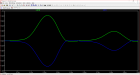
I tried 100pF, 50pF, 22pF from base of predriver on negative side to ground and found out the best setting is no filter in that place. Here is the scope shot. Slight deviation on the scope I think due to cheap Chinese probe without working compensation feature. Also the oscillation spikes from touching by DMM leads voltage terminals or other parts of the board disappeared. After 10 min of work and heatsink warm up, they appeared again but with less intensity. This is what happens when I measure the voltage at front end part of the amp. The last two pictures. The scale on the second picture is little more wider (perhaps two times) than on first picture on the 20nS setting.
So, my choice of compensation capacitors are 8pF on the VAS transistors, 100pF on predrivers and without RC fitter. However, at VAS I suspect compensation capacitor works better just on B-C of TO-126 transistor only, where it's now, but I still have to confirm this with the scope.
Now the change of bias current of output transistors doesn't affect the picture on the scope, thus the behavior of the amp.
More test results will follow.
Attachments
![20171226_152519[1].jpg](/community/data/attachments/603/603141-644e0b0885f819d8f0b0ad0bee078638.jpg?hash=ZE4LCIX4Gd)
![20171226_155758[1].jpg](/community/data/attachments/603/603199-5a2650f761a32ef74a6ebbe438a2a9a6.jpg?hash=WiZQ92GjLv)
![20171226_155834[1].jpg](/community/data/attachments/603/603207-e247486f33c6d9bd7afa8ae0dc1edad4.jpg?hash=4kdIbzPG2b)
Last edited:
I've checked my power supplies for oscillation. Here are the results. Perhaps or more likely this is due to long cables I'm using. First is main PSU 32V, second - front end PSU 42V.
Today I aplied the compensation solution described to second channel with Vbe multiplier biasing of output devices. (first channel was with diodes string) and I have to left 100pF capacitor from negative side predriver base to gnd to achieve more flat signal on the scope.
Also the amplifier has a motorboating issue in cold start, which disappears after touching the voltage terminals by dmm leads or lowering output bias current. Maybe this is due to oscillations in PSUs. As well, predrivers are much more hotter than in first channel with diodes string, big VAS transistors are almost cold.
Attachments
![20171227_133739[1].jpg](/community/data/attachments/604/604840-c683c94aab25bebffbf8963ac1e1e1c7.jpg?hash=xoPJSqslvr)
![20171227_133752[1].jpg](/community/data/attachments/604/604849-e00f5da1dc5d2366bf81d9b9707cadc0.jpg?hash=4A9dodxdI2)
Last edited:
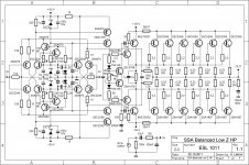
Where are physically located Supply bypassing capacitors? -
(C28,C30,C32,C29,C31,C33) And where is physically return path to ground from these capacitors?
Regarding compensations - the best way for stability (but not the best for high speed performance) to use one compensation (on The VAS), but not as many as You can, for example here in the circuit there are many 50pF BC capacitors, maybe they are making almost the same phase shifts and You have parasitic oscillations.
If You want a multi-pole compensation - it is not as simple as it looks.
Also it was a good comment:
I did not find where is showed this 180 degree phase shift, but if it is true - it should oscillate. Also this oscillation could cause the high frequency fluctuations in power supply rails if there is plenty demand of current. Are the Output stage transistors getting hot after a while? If You are not using Zobel at the output - maybe You use dummy load resistor for these tests?As I see, the 180 degree frequency is approx 3MHz. At this frequency, the gain is approx 12dB.
In other words, it should be oscillating.
The capacitors are directly between output transistors. Return path for them between these capacitors. You can check the layout in first post.
I will update the schematic regarding compensation, it has changed, according to my last posts.
Perhaps Hurtig calculated the 180 degree phase shift.
I'm using Zobel filter, it's in the schematic. For tests I'm using 4R speaker driver. Output transistors become hot if I set high bias current for them or due to prolonged oscillation condition without heatsink (in seconds before power cut off), otherwise they are cold.
Last edited:
Thanks Keantoken, very appreciate your efforts.
What way it produces the output or do you mean it doesn't work with negative input pair? The schematic has been changed a little, thanks to Johnego valuable advices. Please check this file. There shouldn't be oscillation on the output, according to my scope.
What way it produces the output or do you mean it doesn't work with negative input pair? The schematic has been changed a little, thanks to Johnego valuable advices. Please check this file. There shouldn't be oscillation on the output, according to my scope.
Attachments
Last edited:
I would have thought at some stage the separate complementary input halves would come together to form a Class A stage ahead of the driver and power outputs.
Looking at the current flows through R39 and R40 see and judge for yourself if this is what you see.
While the input halves operate in push- pull it seems you have taken this idea a stage further with your bias network.
Looking at the current flows through R39 and R40 see and judge for yourself if this is what you see.
While the input halves operate in push- pull it seems you have taken this idea a stage further with your bias network.
Attachments

Looking at the current flows through R39 and R40 see and judge for yourself if this is what you see.
While the input halves operate in push- pull it seems you have taken this idea a stage further with your bias network.
Could you please elaborate what these graphs mean in terms of sound? I'm sorry, but I don't understand them.
Could you please elaborate what these graphs mean in terms of sound? I'm sorry, but I don't understand them.
R39 and R40 indicate your voltage amplifier stage has a hiatus at the midpoint where there is next no current for nearly 0.1 mS so this is operating in a non-linear way.
For a linear outcome the current needs to be constant with little movement around a fixed point - datasheets will show that transistors have some slope whereas increasing smaller segments on a slope will more closely resemble a straight line.
The gain of a voltage amplifier stage depends on the load on the collector in k ohms and the current in mA times Gm which for transistors is approximately 40.
There is an upper limit to this however it will be apparent the gain has a free spirit to roam without much control with the varying current.
Apart from this there are stored charges in the base area of a power transistor that need to be cleared out before it can be turned off and the process of doing this is delayed by nearly 0.1 mS due to the fact the voltage amplifier delivery on hold.
Large varying currents are the domain of the driver and output transistors. You need to change your voltage multiplier so it runs in Class A - a conventional single transistor will be fine and that would be my recommendation as a first step. At a guess 10 mA through this stage might be a starting point.
If you are insistent on having two transistors - then check out this link
Adcom GFA-535 - Manual - Stereo Power Amplifier - HiFi Engine which is rumoured to have been the design work of Nelson Pass.
You need to change your voltage multiplier so it runs in Class A - a conventional single transistor will be fine and that would be my recommendation as a first step. At a guess 10 mA through this stage might be a starting point.
If you are insistent on having two transistors - then check out this link
Adcom GFA-535 - Manual - Stereo Power Amplifier - HiFi Engine which is rumoured to have been the design work of Nelson Pass.
Thank you for your explanation.
Could you please show your recommendation in appropriately changed sim file?
Removing R39, R40 won't help?
It's all in the VAS stage and the value of the capacitor from the base to collector primarily in theory and simulations. But PCB layouts are now a forgotten art, which alas, only experience will teach you.
Thank you for your explanation.
Could you please show your recommendation in appropriately changed sim file?
Removing R39, R40 won't help?
We can leave these till later in the meantime use Kean's simulation as a compass as the component values you have used are inter-dependent and changing one or two will impact further down the conduction chain.
You have to find the point in your circuit where the hiatus originates by tracing the currents in the small signal stage - for instance R3 and R10 both 10R in value are passing too much current.
You will lose some voltage gain as a consequence of increasing the value of these resistors but you have too much voltage gain in this section to start with and so doing will obviate the hiatus resulting in a low level sine wave at the output which is what should be expected.
Most of the gain is a function from the voltage amplification stage around which the dominant compensation is arranged.
Do you mean R3 and R5 emitter resistors are passing 60mA each and another pair R17, R18 are passing 100mA each, according to simulation? In fact first pair are passing about 3mA and second pair about 3.6mA. These currents, as well as output offset, are set by R8, R9 POTs. Minimum recomended currents through emitter resistors are at least 3mA
Last edited:
Do you mean R3 and R5 emitter resistors are passing 60mA each and another pair R17, R18 are passing 100mA each, according to simulation? In fact first pair are passing about 3mA and second pair about 3.6mA. These currents, as well as output offset, are set by R8, R9 POTs. Minimum recomended currents through emitter resistors are at least 3mA
You are right I did mean R3 and R5 which I changed to 910R to close the gap.
As I mentioned all the component values are interdependent and in consequence of increasing these values less current is drawn across R7 and R6 and the voltage drop across these is reduced to the point where the emitter to base of voltage between the base of Q14 and Q16 is reduced to 0.04V which is below the conduction threshold.
You can see this in attachment - I have indicated the tool I used in my simulations with a red arrow.
I could not find a happy medium by substituting resistor values and the solution to the problem could involve changes to the circuit structure. There are contributors who like challenges of complex circuits - in such company I am happy to to retreat to the ranks of the spectators.
Attachments

I see where you derived this circuit from - see the attachment in your post 51. No need to ask for help with sorting out the modifications you added just go back to the attachment and if you want to run balanced input lines devise a separate in inline circuit for that purpose ahead of your power amplifier.
The original circuit this one. As you can see, I only reduced the output devices and voltage rails. Why the current flow via R17, R18 is not equal to R3, R5 pair?
Do you think this schematic is not correct? Perhaps Q14 or Q16 with lower beta may be of help?
Do you think this schematic is not correct? Perhaps Q14 or Q16 with lower beta may be of help?
Attachments
Last edited:
- Home
- Amplifiers
- Solid State
- One of the Top Solid-State CFA amp design