jgedde said:All,
I have started temperature testing of JPV's 3xxx series ThermalTrak diodes. -25 is complete. What I can tell you at this point is that it appears the diodes in 3xxx are definitely not the same as those in the 4xxx series...
The -25 curve agrees very well with the curve in the NJL3281/1302 datasheet. I was succesful in modifying the test setup to collect data down to 100 uA...
John
Excellent work John.
Does anyone in this thread have any contacts at ONsemi? You would think they would tell us this sort of thing without us having to find it out the hard way. After all, this thread is very likely the cutting-edge of TTrak application.
I wonder if anyone at ONsemi is reading it?
ONsemi can't be bothered to correct errors in their datasheets, even when we tell them the mistakes.
Why should they bother to read up on real data on their devices?
Now, if I were to send this post to their QA director!
Who knows who he/she is?
Why should they bother to read up on real data on their devices?
Now, if I were to send this post to their QA director!
Who knows who he/she is?
DouglasSelf said:
Does anyone in this thread have any contacts at ONsemi? You would think they would tell us this sort of thing without us having to find it out the hard way.
I do and I'll pass the info along, but don't hold your breath for any short term improvements.
But what errors? The 4xxx data I collected agrees with the datasheets within reasonable limits.
The 3xxx data seems to be close as well, but I haven't looked closely enough yet to say there are indeed errors in the diode curves.
John
The 3xxx data seems to be close as well, but I haven't looked closely enough yet to say there are indeed errors in the diode curves.
John
jgedde said:But what errors? The 4xxx data I collected agrees with the datasheets within reasonable limits.
The 3xxx data seems to be close as well, but I haven't looked closely enough yet to say there are indeed errors in the diode curves.
John
John that is good news.
When you do the Vbe tempco on the transistor with constant current, could you do that at Ic = 250mA as well as 100mA?
Stinius
A thought strikes. (Happens sometimes) It seems to me we may have been assuming a bit too quickly that the sensing diodes are isothermal with the transistor junction, and that all we need to do is find a way to match the tempcos and all will be well. As I understand it, all we know about the internals is that the diode is mounted on the other side of the metal plate that contacts the outside world.
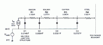
Considering that I have been responsible for ordering 100,000s of power transistors, it occurs to me that I am lamentably ignorant about the details of their internal construction. Back in the day when I was doing the thermal simulations in Chapter 13 of my slim monograph http://www.dself.dsl.pipex.com/ampins/books/book.htm I got some data about the MJ15023 (TO-3) from Motorola Toulouse. The picture below shows the figures for the internal thermal resistances and thermal masses that they gave me, scaled so they can be put straight into a SPICE simulator.
Apparently the silicon die was soldered to a copper header that in turn was welded (?) to the steel TO-3 flange.
The TTrak devices are obviously plastic, but it seems plausible that once more the die is soldered to the metal plate that we can see, and that the diode die is soldered to the same plate in a different operation and using a different blob of solder. That means (refer to the picture) that there will be a temperature drop in the body of the transistor silicon, and another in the transistor mounting solder, which means the diode will never be at the junction temperature.
There is now no steel flange, so there is just the thermal resistance of the thermal washer between the copper part and the heatsink. A rough calculation gives me 1 degC/W for a TO-264 washer of the standard material.
Taking the values from the picture, in the absence of any other data, the total resistance between junction and metal plate is 0.164 degC/W. Treating that as a resistive divider with the washer resistance, and assuming the heatsink does not change in temperature during the timescales we are interested in, that means that the sense diode can never reach more than 86% of the transistor junction temperature.
This does not explain why I needed four effective diodes rather than two to get the compensatiion right- a figure of 50% would be needed for that. But it is a thought.
This is of course a very simplistic model, and ignores other heat paths inside the package. We know these exist, because the top of the package gets hotter than the adjacent heatsink. But what are they? Does anyway know anything more about the internal construction of the TTrak devices? Are the transistor and diode in a little hollow in the plastic, or what?
Attachments
DouglasSelf said:Does anyway know anything more about the internal construction of the TTrak devices? Are the transistor and diode in a little hollow in the plastic, or what?
I may know a thing or two 😀
Conceptually, the same equivalent schematic you got from Motorola applies for the NJL; all decent power devices (be it in TO3, TO247 or TO218, fakes not included) are mounted using what is called a "copper pre-form". Now, the values for the elements are generally not exactly known and no semiconductor manufacturer is going to oficially reveal and guarantee such parameters. What you got is most likely the result of some calculations, simulations and estimates for TO3.
I may crack a new NJL device, but last time I've checked the diode is not mounted using a copper preform, (this would connect the diode substrate to the collector; also copper preforms are expensive in terms of mass production) but using insulating epoxy. Which makes the thermal series resistance much larger than the transistor silicon-preform stack. Therefore, it is safe to assume there is a significant temeperature gradient between the transistor chip and the diode chip. How large, it is hard to say, only some calculations could be made... My estimate (based on other devices I worked with) is 10-15%
Look at these NJL devices as the best of the worlds in terms of temperature tracking; the Sanken devices are a little bit more elaborated but they are essentially not that much better. The ultimate device would have to be built with on chip, dielectrically insulated, diode but I certainly doubt this will ever be in production due to the economics. A separate diode chip is almost free, while an integrated, dielectrically insulated diode will most likely double the cost of the transistor itself. Add to this the lack of flexibility (OnSemi is selling the same transistor chips but without the diode, in the three pin TO218, as the MJL series) to understand why we are probably never going to get the goodies we are hoping for. All we can do is to understand how these devices are working and hence how to use them to our best. In this sense, what John is doing is very good stuff.
Douglas
This is an interesting thought.
Have you tried to contact Charles Hansen? He is a member here and has a lot of knowledge on the TT devices. He also knows the designer of the TT and other people at ONsemi.
I’m sure that I don’t have to mention it but he designed the Ayre amp that uses TT devices.
By the way has anybody heard something from him lately?
How is he doing after the accident? I hope everything is ok.
Stinius
Hmmmm. Maybe I can have one X-rayed. We use x-ray for inspection of MIL and space BGA soldering and PCB vias.
Or at least put one on the old Bridgeport and mill the plastic. JPV, don't worry. I'll use mine...
John
Or at least put one on the old Bridgeport and mill the plastic. JPV, don't worry. I'll use mine...
John
Yes, I believe you are right. That's why I think this whole thread is a bit misguided trying to just match their temperature coefficient. Measuring the real thing is what counts as always 😀
Thermal trak diodes will be measuring something closer to case temperature than junction temperature - but this is still very good compared to measuring heatsink temperature. Don't know how much better than a top mounted transistor it is though, but maybe a bit as thermal conduction through the epoxy is probably not as good and fast.
Also there is a positive feedback mechanism which causes some extra temperature dependency of bias current if temperature sensor doesn't measure junction temperature: Increased junction temperature leads to increased bias current which also leads to increased power dissipation and so on...
Are you sure the model you posted is correct though? It has only 0.284 of total thermal resistance, but maybe it uses som other scaling between power dissipation and model current than 1W <-> 1A. But still you are right, transistor junction will be at much higher temperature than the copper baseplate. It's probably better if the diode is mounted near above the chip than on the baseplate.
It would be interesting to know where the diode is. Is it above the chip in the epoxy or is it down against the back of the transistor? The plastic packages are usually made with the chip soldered directly to the back plate which is already copper unlike in TO3 where it is steel. This is probably the reason why plastic packages have better thermal resistance than TO-3. (Steel doesn't conduct heat that well)
jgedde said:Hmmmm. Maybe I can have one X-rayed. We use x-ray for inspection of MIL and space BGA soldering and PCB vias.
Or at least put one on the old Bridgeport and mill the plastic. JPV, don't worry. I'll use mine...
John
John
I think a lot of people in here will send a new TT.
You are doing a very good job.
Stinius
DouglasSelf said:
Excellent work John.
Does anyone in this thread have any contacts at ONsemi? You would think they would tell us this sort of thing without us having to find it out the hard way. After all, this thread is very likely the cutting-edge of TTrak application.
I wonder if anyone at ONsemi is reading it?
Douglas, First off let me say it is indeed an honor to be corresponding with the fellow who wrote "the book" that kicked of my diyaudio-ing.
They really have told us... The datasheets, which seem to be more or less correct, have the diode curves we need. The curves in the 4xxx datasheet are not the same as in the 3xxx datasheet and I have verified that they are indeed different. I wonder why OnSemi chose a different diode? Looks like the 4281/4302 has the potential for better tracking at normal Vas currents. Maybe that's why. How long did OnSemi take to introduce the 4xxx series after they introduced the 3xxx series?
In all honestly, I would have never undertaken this exercise if list members hadn't doubted the datasheets. I would have taken the datasheet as gospel, at least until a circuit didn't work forcing me to dig further.
Nonetheless, this hasn't been a fruitless exercise... The models Onsemi provides for the diodes are only a loose approximation of the truth. I would be left forever wondering whether the datasheet is right or whether the SPICE model is right.
That said, I have not yet been successful in tweaking the SPICE model for the 4xxx diodes to reflect what I have measured. Whn plotted on a log scale for current, linear scale for voltage, a simulated VI curve using the OnSemi model plots a straight line, not the second order looking curve of my measurements....
Cheers,
John
"That said, I have not yet been successful in tweaking the SPICE model for the 4xxx diodes to reflect what I have measured. Whn plotted on a log scale for current, linear scale for voltage, a simulated VI curve using the OnSemi model plots a straight line, not the second order looking curve of my measurements.... "
John
With all the data you have now it should be possible to make a new model of the diode or just confirm that the OnSemi model is correct.
Maybe Andy C could do something?
Stinius
John
With all the data you have now it should be possible to make a new model of the diode or just confirm that the OnSemi model is correct.
Maybe Andy C could do something?
Stinius
jgedde said:
That said, I have not yet been successful in tweaking the SPICE model for the 4xxx diodes to reflect what I have measured.
Sounds like it's time for CurveCaptor -- which some of the tubies use.
I believe it is time to make a summary.
The initial question was: the temco of the diode and of the Vbe of the transistor are not the same for the 3XXX serie at normal bias current in the diode ( whatever this means)
It seems that looking at the datasheet of the 4XXX, the tempcos are the same around 10mA in the diode.
My opinion is:
We need to know the Vbe tempco of the transistors at constant Ic collector current of 100mA for operating temperatures between 25 and 75 °C. It is supposed to be 2.1mV/°C but should be known accurately.
If there is a difference in temperature between the two junctions this difference is proportional to the temperature and can be compensated in the tracking by increasing the tempco of the diode. Therefore, beeing able to adjusting the tempco of the diode is important whatever the type
It is therefore important to have an accurate view of the variation of tempco of diode with current to understand if adjustment is possible. For the 3XXX serie it seems that we have to go very low in current to have the right tempco ( if possible )
Questions:
The measurements of the diode in the 4XXX model are not showing the increase in tempco with decrease of current. The data sheet on the contrary shows this correctely.
The results from Douglas ( higher Vbe multiplication and higher tempco required) remains unexplained.
JPV
syn08 said:
I may know a thing or two 😀
Conceptually, the same equivalent schematic you got from Motorola applies for the NJL; all decent power devices (be it in TO3, TO247 or TO218, fakes not included) are mounted using what is called a "copper pre-form". Now, the values for the elements are generally not exactly known and no semiconductor manufacturer is going to oficially reveal and guarantee such parameters. What you got is most likely the result of some calculations, simulations and estimates for TO3.
I may crack a new NJL device, but last time I've checked the diode is not mounted using a copper preform, (this would connect the diode substrate to the collector; also copper preforms are expensive in terms of mass production) but using insulating epoxy. Which makes the thermal series resistance much larger than the transistor silicon-preform stack. Therefore, it is safe to assume there is a significant temeperature gradient between the transistor chip and the diode chip. How large, it is hard to say, only some calculations could be made... My estimate (based on other devices I worked with) is 10-15%
Look at these NJL devices as the best of the worlds in terms of temperature tracking; the Sanken devices are a little bit more elaborated but they are essentially not that much better. The ultimate device would have to be built with on chip, dielectrically insulated, diode but I certainly doubt this will ever be in production due to the economics. A separate diode chip is almost free, while an integrated, dielectrically insulated diode will most likely double the cost of the transistor itself. Add to this the lack of flexibility (OnSemi is selling the same transistor chips but without the diode, in the three pin TO218, as the MJL series) to understand why we are probably never going to get the goodies we are hoping for. All we can do is to understand how these devices are working and hence how to use them to our best. In this sense, what John is doing is very good stuff.
Hi
I am confused. What is a copper preform? Is it something that goes between the die and the metal plate? If so what holds it all together?
If the diode is mounted using insulating epoxy, that doesn't affect the rough calculation I did in the steady state, providing there is no significant heat loss from the diode. But there may be- this is why I would like to know the construction details. Certainly epoxy rather than solder would increase the time-lag.
I fear that to get a real feel for this we need a proper Finite Element Analysis of the package, and to do that we would need more data about the device than we are ever likely to get.
Does anyone know of a freeware FEA package? They do exist, because I was sent one, but the instructions are in Russian...
If you Google Mr Self you'll find stuff about copper preform. I just didDouglasSelf said:Hi
I am confused. What is a copper preform?

JPV said:I believe it is time to make a summary.
The initial question was: the temco of the diode and of the Vbe of the transistor are not the same for the 3XXX serie at normal bias current in the diode ( whatever this means)
It seems that looking at the datasheet of the 4XXX, the tempcos are the same around 10mA in the diode.
My opinion is:
We need to know the Vbe tempco of the transistors at constant Ic collector current of 100mA for operating temperatures between 25 and 75 °C. It is supposed to be 2.1mV/°C but should be known accurately.
If there is a difference in temperature between the two junctions this difference is proportional to the temperature and can be compensated in the tracking by increasing the tempco of the diode. Therefore, beeing able to adjusting the tempco of the diode is important whatever the type
It is therefore important to have an accurate view of the variation of tempco of diode with current to understand if adjustment is possible. For the 3XXX serie it seems that we have to go very low in current to have the right tempco ( if possible )
Questions:
The measurements of the diode in the 4XXX model are not showing the increase in tempco with decrease of current. The data sheet on the contrary shows this correctely.
The results from Douglas ( higher Vbe multiplication and higher tempco required) remains unexplained.
JPV
I agree in your summary, but to make a conclusion we have to wait for the data from John.
Regarding the Vbe measurements I think it would be good to do the measurements with more than one constant collector current. If the measurements could be done in 10mA steps from 50mA – 300mA we would have much more data to compare. We could also look at different values of Re.
Stinius
stinius said:
I agree in your summary, but to make a conclusion we have to wait for the data from John.
Regarding the Vbe measurements I think it would be good to do the measurements with more than one constant collector current. If the measurements could be done in 10mA steps from 50mA – 300mA we would have much more data to compare. We could also look at different values of Re.
Stinius
Ok the more date the better. But what we realy need is the Vbe drift around 100mA. The tempco coefficient is changing by 0.2mV/°C per decade of current. Therefore, if we know it at 100 mA the drift mill be nearly the same at other realistic currents.
The Vbe change at constant temperature should be 60mV per decade of current.
JPV
- Status
- Not open for further replies.
- Home
- Amplifiers
- Solid State
- On Semi ThermalTrak