Dia attach:
A silicon die is brazed or soldered to a baseplate.
Braze is either gold-germanium at 345 C, or gold-tin at 280 C, bot eutectics. (don't hang me on the 345, it's been 15 years)..
Many times, the baseplate is inadequate as a spreader, it will confine the heat transfer to the heatsink to the die size plus twice the baseplate thickness (the 45 degree model is usually within 10% of reality) a 50 mil thick spreader increases the thermal footprint by 100 mils in both directions, this is a big jump when the die is 100 to 150 mils to a side.
Solders, there are many, and many melt temps..
From the junction on the top, through the silicon from 15 to 20 mils thick, through a die attach solder (started as a preform), to the copper heat spreader, through a braze (again, a preform), to the baseplate.
Cheers, John
All,
Here are the diode temperature curves for the NJL3281 and 1302. Note that I didn't perform the testing at as many temperatures as I did for the 4281/4302. This is for two reasons:
1) They agree with the datasheet about as well as the 4281/4302
2) Time constraints.
Now, onto Vbe tempco testing on all 8 at Ic=0, and Vbe tempco on a single representative sample at Ic=100mA...
Cheers,
John
Attachments

DouglasSelf said:
So far as I can tell I am the only one who has built and measured a TTrak amplifier so far.
Not the only one. See:
RMI-FC100 schematic
in this thread:
RMI-FC100 thread
Also, Charles Hansen might have a commercial embodiment. In any event, he has looked at them and discussed their characteristics:
ThermalTrak thread
pooge
I think Douglas is talking about the measurements he has done, and that he is sharing with the rest of us.
I’m sure Chales has done some measurements as well, but I don’t think he will share them.
Stinius
I think Douglas is talking about the measurements he has done, and that he is sharing with the rest of us.
I’m sure Chales has done some measurements as well, but I don’t think he will share them.
Stinius
pooge said:
Not the only one. See:
RMI-FC100 schematic
in this thread:
RMI-FC100 thread
Also, Charles Hansen might have a commercial embodiment. In any event, he has looked at them and discussed their characteristics:
ThermalTrak thread
Thanks for alerting me to that thread. It's good to see people getting stuck in and building.
However, I have just skimmed through the whole thread and there appear to be no measurements at all, and virtually no reference to the correctness or otherwise of the thermal dynamics.
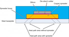
Here's a drawing of a typical device.
Can anybody tell me where the diode is located? Is it on the spreader, on the baseplate, or on the top of the silicon?
I also show the heat path difference, and this is the reason for the copper spreader, to reduce the heat flux density through the heatsink compound, and reduce the theta JC..
Note...the lines are the 45 degree lines of the heat spread model.
Cheers, John
Attachments
jneutron said:Here's a drawing of a typical device.
Can anybody tell me where the diode is located? Is it on the spreader, on the baseplate, or on the top of the silicon?
I also show the heat path difference, and this is the reason for the copper spreader, to reduce the heat flux density through the heatsink compound, and reduce the theta JC..
Note...the lines are the 45 degree lines of the heat spread model.
Cheers, John
This is what charles Hansen is writing in another thread:
they take a MUR120 (sans the epoxy body) and mount it to the copper lead frame near the transistor die. The resulting product has less than 2 pF of capacitance between the transistor and the diode.
Stinius
Hmmm..we're gonna need a looksee into the device.stinius said:
This is what charles Hansen is writing in another thread:
they take a MUR120 (sans the epoxy body) and mount it to the copper lead frame near the transistor die. The resulting product has less than 2 pF of capacitance between the transistor and the diode.
Stinius
If the die is on the copper lead frame, then it is outside the 45 degree cone. If you have a really good thermal interface between the leadframe and the heatsink, the diode will never get to the die temperature, and there will be a considerable thermal lag.
That may explain why it takes twice as many diodes to achieve real tracking. And why devices in the oven look ideal.
If you use a very bad heatsink to leadframe interface, the diode will probably track better. Like, dry mounting the device without compound..
YO neighbor: any chance of x-raying the device? Is charles talking about a diode with actual leads and glass passivation, or is it a chip with wirebonds?
Cheers, John
jneutron said:Here's a drawing of a typical device.
Can anybody tell me where the diode is located? Is it on the spreader, on the baseplate, or on the top of the silicon?
I also show the heat path difference, and this is the reason for the copper spreader, to reduce the heat flux density through the heatsink compound, and reduce the theta JC..
Note...the lines are the 45 degree lines of the heat spread model.
Cheers, John
Thanks for that, but what is it a drawing of? The devices we are talking about have a plate of copper connecting with the outside world, though it does have a silvery coating, possibly nickel???
(Moment of doubt. Pause to scrape coating off a 2SA1302- yes it's definitely copper under there. I'm not going to do it to one of my precious TTraks, but I think it is a safe call that they are copper too- they're certainly not magnetic)
Perhaps your drawing is of a TO-3? Modern ones have steel flanges, as a moment with a magnet demonstrates; for example:
MJ21193, MJ21194 have steel flanges
MJ15024, MJ15025 have steel flanges
MJ15001, MJ15002 have steel flanges
DouglasSelf said:
Thanks for that, but what is it a drawing of? The devices we are talking about have a plate of copper connecting with the outside world, though it does have a silvery coating, possibly nickel???
(Moment of doubt. Pause to scrape coating off a 2SA1302- yes it's definitely copper under there. I'm not going to do it to one of my precious TTraks, but I think it is a safe call that they are copper too- they're certainly not magnetic)
Perhaps your drawing is of a TO-3? Modern ones have steel flanges, as a moment with a magnet demonstrates; for example:
MJ21193, MJ21194 have steel flanges
MJ15024, MJ15025 have steel flanges
MJ15001, MJ15002 have steel flanges
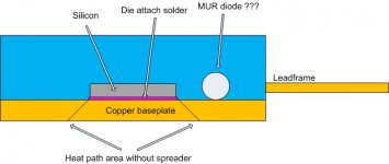
From the discussion, there was mentioned a copper something and a steel baseplate. I drew exactly that.
Is it more like this??
Attachments
NJL3281/1302 Vbe tempco data. Ic=0.
NPN tempco:
-2.53mV/ºC @ 100µA
-2.26mV/ºC @ 1mA
-2.06mV/ºC @ 10mA
-1.71mV/ºC @ 100mA
PNP tempco:
-2.51mV/ºC @ 100µA
-2.26mV/ºC @ 1mA
-2.05mV/ºC @ 10mA
-1.69mV/ºC @ 100mA
Cheers,
John
NPN tempco:
-2.53mV/ºC @ 100µA
-2.26mV/ºC @ 1mA
-2.06mV/ºC @ 10mA
-1.71mV/ºC @ 100mA
PNP tempco:
-2.51mV/ºC @ 100µA
-2.26mV/ºC @ 1mA
-2.05mV/ºC @ 10mA
-1.69mV/ºC @ 100mA
Cheers,
John
jgedde said:NJL3281/1302 Vbe tempco data. Ic=0.
NPN tempco:
-2.53mV/ºC @ 100µA
-2.26mV/ºC @ 1mA
-2.06mV/ºC @ 10mA
-1.71mV/ºC @ 100mA
PNP tempco:
-2.51mV/ºC @ 100µA
-2.26mV/ºC @ 1mA
-2.05mV/ºC @ 10mA
-1.69mV/ºC @ 100mA
Cheers,
John
John thank you very much.
Could you also do the x-ray?
Stinius
jneutron said:
From the discussion, there was mentioned a copper something and a steel baseplate. I drew exactly that.
Is it more like this??
Yes I think it’s more like that.
Anyway it’s outside the Thermal “transmission line” I it’s something that is called that, but I guess you understand what I mean.
Stinius
jneutron said:
From the discussion, there was mentioned a copper something and a steel baseplate. I drew exactly that.
Is it more like this??
I'm pretty sure almost all plastic devices use copper baseplates. Some, like the 2SC3264 in the huge MT-200 has an internal spreader looking like a TO3-P though. It seems the collector lead is usually attached to the baseplate from the beginning too on most devices.
I can see why it is needed in the steel (doesn't conduct heat well at all!) TO-3:s but with copper baseplate I don't know if it is much point, heat conduction through the commonly used insulating pad isn't too good which should mean improving the lateral thermal resistance won't help that much. But I'm not sure - I don't know what the typical thermal resistance from one end of a package to the other is.
Wouldn't that 45-degree thing you shown only be valid for materials with similar heat conductivities?
From http://en.wikipedia.org/wiki/Thermal_conductivity in W/(m*k)
Stainless steel 12.11 ~ 45.0
Lead 35.3
Aluminium 200
Gold 318
Copper 380
Copper is about 8-30 times better than steel!
I 've just had a quick look at what's on the Web about SPICE thermal simulation. If you're interested, there are these papers. I haven't read them, so no guarantees on quality.
The Vishay stuff looks interesting: The last link leads to "Estimating Junction Temperature by Top Surface
Temperature in Power MOSFETs" which sounds promising.
http://www.eetasia.com/STATIC/PDF/200805/EEOL_2008MAY08_POW_EMS_EDA_AN_01.pdf?SOURCES=DOWNLOAD
http://www.vrg.utoronto.ca/~ngwt/Advanced ElectroThermal.pdf
http://eprint.iitd.ac.in/dspace/bitstream/2074/556/1/noosmos1998.pdf
http://www.vishay.com/mosfets/thermasim/
http://www.vishay.com/docs/73554/73554.pdf
http://www.vishay.com/docs/69993/an834.pdf
megajocke said:
I'm pretty sure almost all plastic devices use copper baseplates. Some, like the 2SC3264 in the huge MT-200 has an internal spreader looking like a TO3-P though. It seems the collector lead is usually attached to the baseplate from the beginning too on most devices.
I can see why it is needed in the steel (doesn't conduct heat well at all!) TO-3:s but with copper baseplate I don't know if it is much point, heat conduction through the commonly used insulating pad isn't too good which should mean improving the lateral thermal resistance won't help that much. But I'm not sure - I don't know what the typical thermal resistance from one end of a package to the other is.
Wouldn't that 45-degree thing you shown only be valid for materials with similar heat conductivities?
From http://en.wikipedia.org/wiki/Thermal_conductivity in W/(m*k)
Stainless steel 12.11 ~ 45.0
Lead 35.3
Aluminium 200
Gold 318
Copper 380
Copper is about 8-30 times better than steel!
The 45 model works quite well for typical constructs of silicon, copper, moly, aluminum, beo and alumina...normal materials I've used for military power hybrids as well as TO packages.
Where it starts to fall apart is when the contact material is significantly lower in conductance, as it starts to form an isothermal. The ultimate isothermal is of course, the oven data John is seeing.
This is exactly what you speak of, and yes, you are thinking correctly.
If the diode is outside of the transmission path, then it makes the oven data inconsistent with high power heatsinked operation, as Douglas is finding.
My statement regarding 6 milliamp operation of the diode is due to the production spread, it is tightest at 6 milliamp..
Cheers, John
FWIW, here is the Vbe tempco for a single unit of NJL3281 at Ic=100mA: -2.42mv/ºC. The unit I picked was "middle of the pack." Not the lowest Hfe, nor the highest...
Since the Hfe varies so much, to support Ic=100mA, the base current will vary from unit to unit. When base current varies, so does the tempco for Vbe. But from the data I've collected, this tempco will typically range from 2.3 to 2.5 mV/ºC (on average) for the 3xxx and 4xxx series when standing at Ic=100 mA (Ib=0.4 to 1 mA).
JPV, on to your characteristic curves...
Cheers,
John
Could you also do the x-ray?
I tried, but the back plate made it difficult to discern what was inside. I'm far from an expert at running the x-ray... The best bet would be to mill the plastic away...
John
- Status
- Not open for further replies.
- Home
- Amplifiers
- Solid State
- On Semi ThermalTrak