I did pull the 4N35 out of it's socket (but when the board was still in the chassis). it looked like one of the pins was bent. so maybe that's it.
Might as well scrub off that ugly brown flux while you've got the board out of the chassis. It's especially visible against the white background. M2x post #3 offers some tips about PCB cleaning.
You could temporarily remove the 0R47 source resistors and replace them with 47R resistors for debug purposes. Now you can run the amp all by itself on the bench, without a heatsink, and attach probes to your heart's content.
I'm assuming they would still need to be 3W resistors?
You can earn your Cub Scout Circuit Design Merit Badge by answering this question yourself. Use Ohm's Law to calculate the current and then remember that the power dissipated in an R ohm resistor, carrying I amperes of current, is equal toI'm assuming they would still need to be 3W resistors?
Power_dissipated = I * I * R
Plug in the numerical values which represent the M2 output stage using R=47.0 ohms, and out pops the required power dissipation.
High school math, applied to our daily lives! Ain't it wonderful! Aren't you grateful you paid attention way back then?
I guess you don't remember me...we've had this discussion about doing math before. Maybe this rings a bell (that's funny).
One of the most attractive 23 year old ladies in my circle of friends, used to say "Just get some man to do it for you!" Apparently this worked quite well. For her. Try it yourself, maybe you'll have success...
Trouble here.
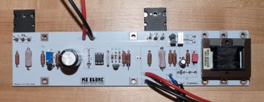
Got the boards soldered up, Tea Bag boards.
Using Toshiba 2SK1530/2SJ201 on the outputs. 2SK1530 in Q1 N Channel, 2SJ201 in Q2 P Channel. Using 0R33 3W source resistors, jumper on R11 as been the go-to values for the Toshiba parts. Using an R20 trim pot for the R3/R4 pair, centered before installing. The 5K trim pot P1 is centered at 2.5K. No short on any MOSFET pin to the heatsink. Both channels do the same thing.
Solder looks fine - I solder everything under a magnifier these days, anyway. Checked all resistor values with a meter before installing them. Verified all part numbers on active devices, socketed optocoupler with dot towards notch on socket/board.
Using a bench supply, the amperage starts off at zero - doesn't move for several seconds, then steadily increases, I set it to stop at 1.25A/21V. DC at the speaker terminals is at 10VDC by that point.
Nothing hot, no smoke, no smells. Something is not right.
Attachments
Last edited:
Using a bench supply, the amperage starts off at zero - doesn't move for several seconds, then steadily increases, I set it to stop at 1.25A/21V. DC at the speaker terminals is at 10VDC by that point.
Nothing hot, no smoke, no smells. Something is not right.
I think this is pretty much normal behaviour. My M2 has BIAS about 1.3A. Are you able to trim DC offset using P1?
hope you didn't current-limited bench supply ; besides that , (just in case) I hope that when you said "installed" - you meant - mounted on heatsink
hope you didn't current-limited bench supply ; besides that , (just in case) I hope that when you said "installed" - you meant - mounted on heatsink
Yes, it was mounted on the heatsink. I didn't set the current limit, but the CL light started blinking as the draw reached 1.25A. I was watching the amp meter and turned it off manually at 1.25A - just as the light started blinking. I think 1.25A is the size of the fuse recommended. What's the upper limit of current draw it can withstand?
And ideas as to why it would have 10VDC at the speaker leads? I didn't try to adjust DC offset with the P1 trimmer, seems like a very long ways from zero and I was concerned about damage to the amp as the current was climbing.
with 0R33 source resistors , amp is going to have higher Iq than 1A25
it is starved now , and it can't settle properly , so your offset reading is irrelevant
I expect that you'll have 1A7 to 1A8 with these source res.
so , connect proper PSU
it is starved now , and it can't settle properly , so your offset reading is irrelevant
I expect that you'll have 1A7 to 1A8 with these source res.
so , connect proper PSU
I can verify for this configuration (schematic as in post #3167) a bias of 1.82 amps (1A82), though my PSU has the rails at +/- 24V.
Best regards, Claas
Best regards, Claas
Last edited:
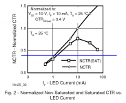
The M2's output MOSFETs operate at a VGS bias of about 5 volts. So with 23 volt supplies, there's about 18 volts across resistor R7 and about 18 volts across resistor R6. (Both are 47K). The current in R6 and R7 is about (18/4.7E4) = 380 microamps. This is also the current in the output half, the phototransistor half, of the 4N35 optocoupler.
The current in the INPUT half of the optocoupler, namely the LED between pins 1 and 2 of the optocoupler, follows the relationship
where "CTR" is the Current Transfer Ratio of the optocoupler. Looking at the datasheet plot of CTR (Figure 1 below), the only way to get I_phototransistor = 0.38mA is to have I_LED = 1mA and CTR=0.4. That's where the blue line intersects the graph.
Finally we look at the I-V plot of the LED. Attached below in Figure 2 is some current-versus-voltage data I measured on the input side (the "LED") of a 4N35 optocoupler made by Vishay. With I_LED = 1mA, the forward voltage drop is about 1.09 volts.
Readers can run through the rest of the algebra involving R10, R11, and R12. And can also calculate the bias voltage across the IC reference voltage "diodes" Q6 and Q7. The result might be surprising.
_
The current in the INPUT half of the optocoupler, namely the LED between pins 1 and 2 of the optocoupler, follows the relationship
I_phototransistor = I_LED * CTR
where "CTR" is the Current Transfer Ratio of the optocoupler. Looking at the datasheet plot of CTR (Figure 1 below), the only way to get I_phototransistor = 0.38mA is to have I_LED = 1mA and CTR=0.4. That's where the blue line intersects the graph.
Finally we look at the I-V plot of the LED. Attached below in Figure 2 is some current-versus-voltage data I measured on the input side (the "LED") of a 4N35 optocoupler made by Vishay. With I_LED = 1mA, the forward voltage drop is about 1.09 volts.
Readers can run through the rest of the algebra involving R10, R11, and R12. And can also calculate the bias voltage across the IC reference voltage "diodes" Q6 and Q7. The result might be surprising.
_
Attachments


Hello,
Does anyone have a recommendation for shielded input cable, available in the US, to use in the M2?
Thanks in advance!
Does anyone have a recommendation for shielded input cable, available in the US, to use in the M2?
Thanks in advance!
I can verify for this configuration (schematic as in post #3167) a bias of 1.82 amps (1A82), though my PSU has the rails at +/- 24V.
Best regards, Claas
Would that be a SMPS?
(referencing the rail voltage of +/- 24V in my M2 build)
No, it's similar to a standard FirstWatt PSU; main deviation is CLC.
Because the wall voltage at my house is more often 220V - 225V AC instead of the specified 230V AC, I use a transformer with 2 x 20V secondaries (500VA audio grade from Toroidy.pl).
Followed by standard rectifier bridges and 66 mF - 2.5 mH - 63 mF CLC PSU.
At my bias current of 2 x 1.82 amps (1A82) (left and right side together give approx.3.64 amps delivered by the PSU), this comes out to about 24V, give and take a few 100 mV, depending on the actual wall voltage. 😉
Best regards,
Claas
Would that be a SMPS?
No, it's similar to a standard FirstWatt PSU; main deviation is CLC.
Because the wall voltage at my house is more often 220V - 225V AC instead of the specified 230V AC, I use a transformer with 2 x 20V secondaries (500VA audio grade from Toroidy.pl).
Followed by standard rectifier bridges and 66 mF - 2.5 mH - 63 mF CLC PSU.
At my bias current of 2 x 1.82 amps (1A82) (left and right side together give approx.3.64 amps delivered by the PSU), this comes out to about 24V, give and take a few 100 mV, depending on the actual wall voltage. 😉
Best regards,
Claas
Last edited:
...interesting bias circuit that you can use elsewhere...
1, Which sounds better, a single pair of output drvices or say 3 deep, biased to the same current; I remember the 'catching fire' quote, if the former, the second question is redundant
2, For multiple output devices, what would be the practicle upper limmit for R13 & R14 without destroying performance; BA2 has 1R, I'm thinking of 1R5.
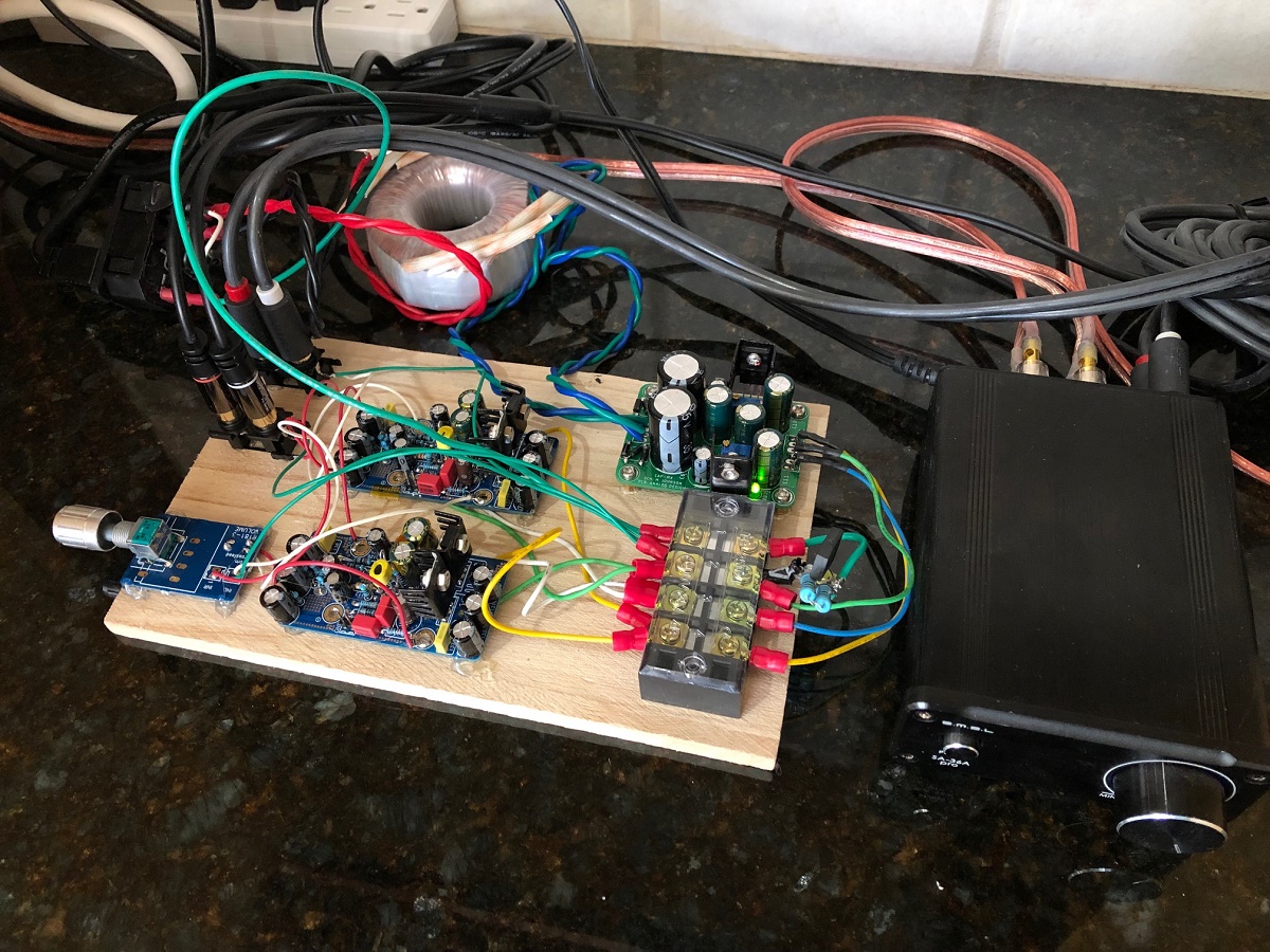
Melbourne tested as standalone preamp, works well. In this wood plank mock up of a preamp, I am using a BJT darlington cap multiplier (layout by Prasi and design by Mark Johnson) to provide +/-17v rails. I am using the built in 2k2 and 220pF input RFI filter in this case. Using star grounding (even audio input and output jacks all go to star hub) which has a 10R/diode bridge/100nF ground loop breaker. System has no audible hum.
Attachments

- Home
- Amplifiers
- Pass Labs
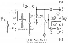
- Official M2 schematic