Voltage at the source of the follower SICFET moves identically to the drain
of the Schaded SICFET, with just enough offset to forward bias the base of
the BJT and let the BJT prevent the follower's gate bias cap further charging.
The load is attached to a resistive voltage divider between output devices.
These measure the class A current total and present it to the BJT for bias
control.
You can get a lower output impedance and higher Mu accuracy by loading
closer to the top of the voltage divider. But reality this does not drive low
impedance loads as well as loading at the center. If it can't swing the full
required current in both push and pull, it matters not what was impedance.
Center best shares the load current swing between the two devices.
This is why I do not agree as-drawn, with load for some reason not center.
Maybe for a 32ohm headphone this makes sense, but not for speakers...
I was under the impression that the imbalance is there to compensate for the impedance at the source. Source impedance + 0.235 = 0.34 Ohms or at least fairly close to it.
Thanks Pico. That would be great. I'm going to put a sine wave through my experiment this evening and take a look with the o'scope. Maybe I can see what is happening.
What Vgs do you need for 1.3A?
What Vgs do you need for 1.3A?
The curve set I ran for this particular device showed that I needed 6 volts Vgs to conduct that current. I checked last night when I had sine generator and scope hooked up and it was exactly that. Interesting finding during test was that gain of channel is way too low. Substituting my Schaded SiCmosfet must have reduced the OLG to a level too low for the gain setting resistors to do their job. The channel was amplifying and the output was distortion free (at least visually), but too little voltage gain compared to the unaltered channel. In listening test I had overdriven the input to clipping (thus the audible distortion ). I was able to reproduce this on the bench. I did try the suggestion to insert blocking cap in Schade inner loop, but could not see much effect. I also tried disconnecting the Schade network completely, and loop gain went up some but not enough to make much difference. I assume that the C2M1000170D is not a good device to substitute for an IRFP240 in the ACA circuit Q1 position, at least not without more adjustments to the design. I guess I can't say that I have it "made in the Schade" as the saying goes...
Thanks to kenpeter and Pico for the explanations . That helps me a lot.
First basic version it will need adjustments to work with C2M1000170D
R3 is probably totally unnecessary
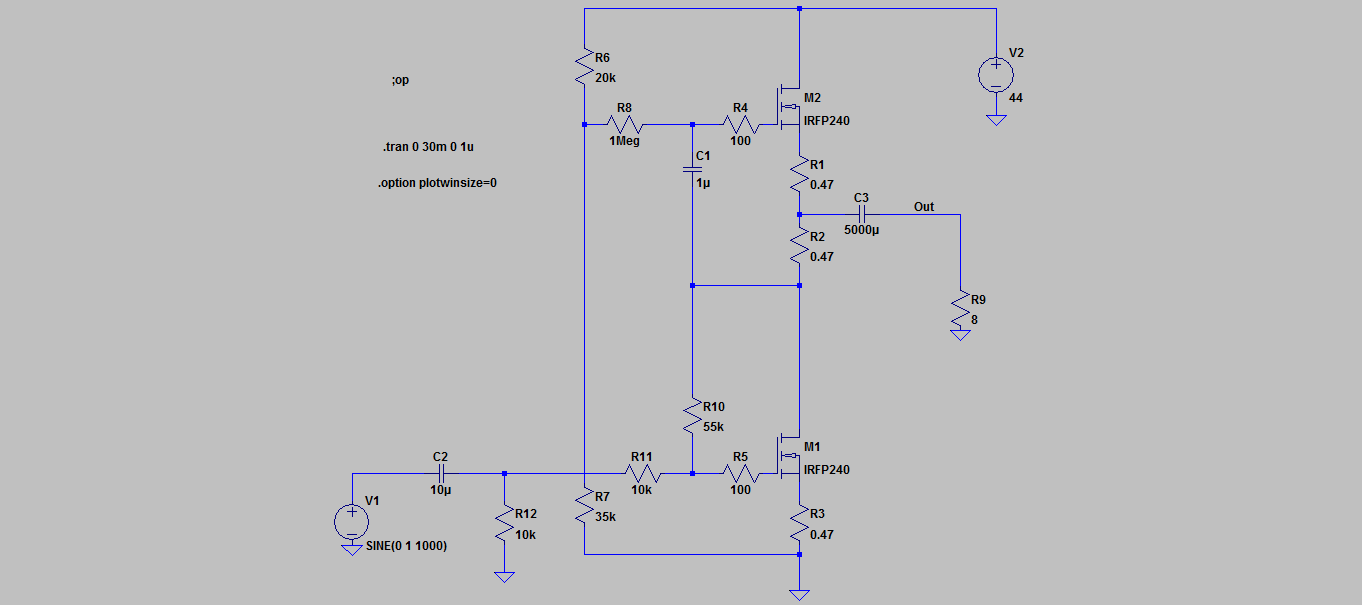
R3 is probably totally unnecessary
Last edited:
R6 and R7 adjust bias point of M2. So you will need a pot.
R10 and R11 schade feedback loop adjust bias point of M1.
Changing source resistor values will also aid in adjusting bias points.
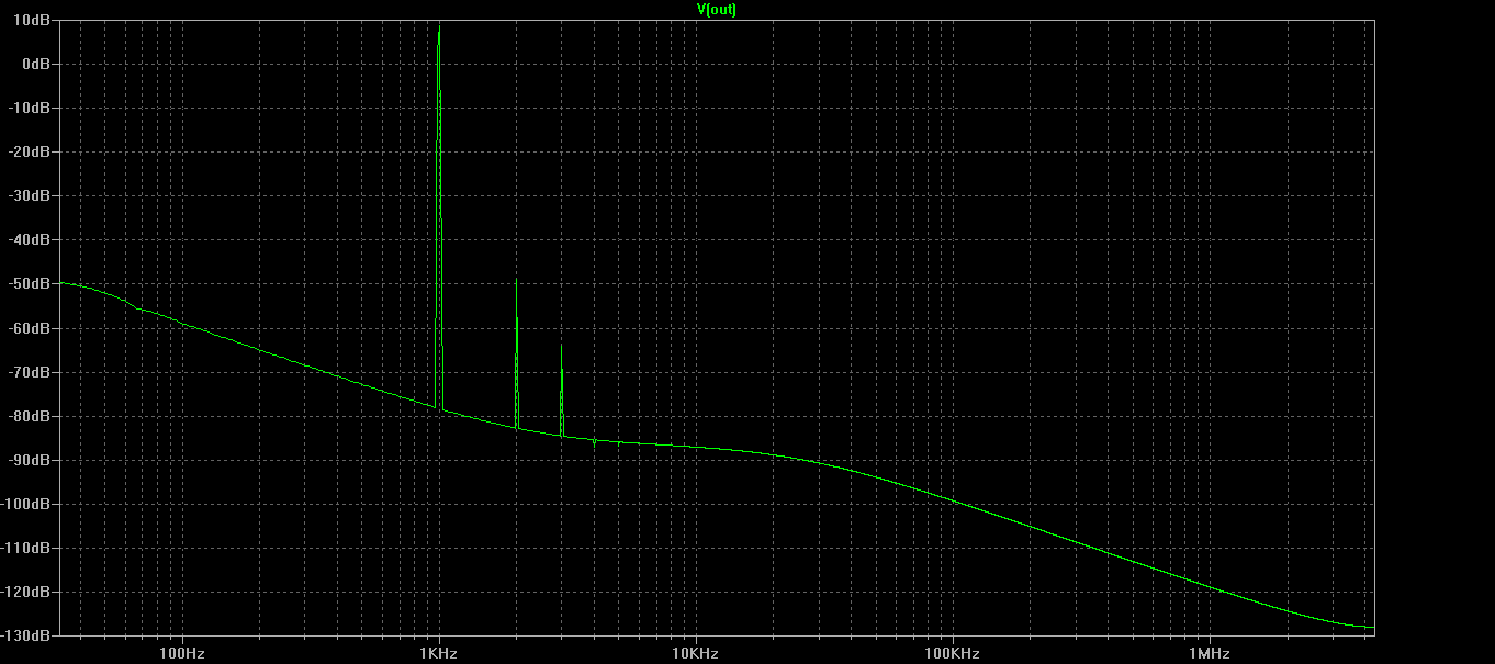
Here is distortion of circuit above. Obviously with IRFP240 bandwidth will be limited but with your device it should be fine
R10 and R11 schade feedback loop adjust bias point of M1.
Changing source resistor values will also aid in adjusting bias points.
Here is distortion of circuit above. Obviously with IRFP240 bandwidth will be limited but with your device it should be fine
Last edited:

I'll try and do one for C2M1000170D (having issues with models), but hopefully this will be enough to get you building something.
I'll try and do one for C2M1000170D (having issues with models), but hopefully this will be enough to get you building something.
That looks pretty straightforward. Thank you very much!
I'll try and do one for C2M1000170D (having issues with models)...
I fought through issues with their models and finally got things working. Are you using the power_nmos_heat symbol? In addition to the usual
Code:
.inc C2M1000170D.libI also found that in most cases adding
Code:
.OPTIONS METHOD=GEAR ABSTOL=1e-6 CHGTOL=1e-12 GMIN=1e-9 ITL1=1000 ITL2=1000 RELTOL= 0.001 VNTOL=1e-3 NOOPITERwas a must. I usually run a 50V source from Tc to ground and a 150V source from Tj to ground to simulate 50C case temperature and 150C junction temp. These are likely too high.
I fought through issues with their models and finally got things working. Are you using the power_nmos_heat symbol? In addition to the usual
Code:.inc C2M1000170D.lib
I also found that in most cases adding
Code:.OPTIONS METHOD=GEAR ABSTOL=1e-6 CHGTOL=1e-12 GMIN=1e-9 ITL1=1000 ITL2=1000 RELTOL= 0.001 VNTOL=1e-3 NOOPITER
was a must. I usually run a 50V source from Tc to ground and a 150V source from Tj to ground to simulate 50C case temperature and 150C junction temp. These are likely too high.
I got it working, but I have no faith in the results.
I will have another go at working with them.
I'm tempted to make my own simplified model.
Wouldn't this circuit https://www.passdiy.com/project/amplifiers/son-of-Zen now coming up to it's 20th anniversary be a great candidate to be Passified? Balanced power triodes anyone?
These power mongering SiCs should be able to flex their muscles here.
These power mongering SiCs should be able to flex their muscles here.
Has the site been cyber attacked.
Getting security warnings.
Not showing on mine...
Wouldn't this circuit https://www.passdiy.com/project/amplifiers/son-of-Zen now coming up to it's 20th anniversary be a great candidate to be Passified? Balanced power triodes anyone?
These power mongering SiCs should be able to flex their muscles here.
I'm only just now contemplating a chokeloaded version and wondering how the schade feedback on the Cree SicFET would go... I've some LU parts as well and the Donut thread pretty much lays the path to follow there, but this looks like fun...
Some 650VA torroids landed in my lap, so there's the chokes, and I bought the Cree fets a while back so It seems tempting to go for it. 🙂
I was under the impression that the imbalance is there to compensate for the impedance at the source. Source impedance + 0.235 = 0.34 Ohms or at least fairly close to it.
Source impedance that high? Even with the BJT feeding back to the gate?
Maybe so with that big cap defeating such feedback. I still suggest a small
resistor tween cap and collector, but whatever...
Again, impedance matters not if push and pull can't swing the same limits.
Equal resistors give the highest limit that both can agree to work with.
Lets not confuse channel resistance with impedance, both push and pull
suffer the same minimum resistance regardless local feedback scheme.
Last edited:
Source impedance that high? Even with the BJT feeding back to the gate?
Maybe so with that big cap defeating such feedback. I still suggest a small
resistor tween cap and collector, but whatever...
Again, impedance matters not if push and pull can't swing the same limits.
Equal resistors give the highest limit that both can agree to work with.
If you go to Nelson's video presentation he discusses a little about resistance values.
I don't think it's worth worrying about too much but it is definitely something you can play around with.
Has the site been cyber attacked.
Getting security warnings.
I get a pop up warning also but I think it is just referring to the secure setting. In chrome I just click go anyway. I do not think there is any problem with a virus or such just maybe ordering and then it just may be the security settings with your virus software or browser. Perhaps Mr Pass should be made aware of this.
I'm only just now contemplating a chokeloaded version and wondering how the schade feedback on the Cree SicFET would go... I've some LU parts as well and the Donut thread pretty much lays the path to follow there, but this looks like fun...
Some 650VA torroids landed in my lap, so there's the chokes, and I bought the Cree fets a while back so It seems tempting to go for it. 🙂
If you've got all the hardware and the space to heat, go for it Aren! Mr. Pass probably has an official circuit up his sleeve...

Oh I shouldn't, but...
Cheers for the encouragement. I can arguably find a matching pair of chassis and power supply bits and pieces as well... It will entail removing a mostly completed F6 from its heatsinks and starting again there...
Edit - Oh hang it. I'll do the grunt work if I can get some help? I dont follow how the schade feedback and not-really-the-gate-stopper-anymore resistor values are derived and how to assess the choke load parameters, but if some one wants to lend a hand?
If you've got all the hardware and the space to heat, go for it Aren! Mr. Pass probably has an official circuit up his sleeve...
Cheers for the encouragement.
I can arguably find a matching pair of chassis and power supply bits and pieces as well... It will entail removing a mostly completed F6 from its heatsinks and starting again there...Edit - Oh hang it. I'll do the grunt work if I can get some help? I dont follow how the schade feedback and not-really-the-gate-stopper-anymore resistor values are derived and how to assess the choke load parameters, but if some one wants to lend a hand?
Last edited:
Wouldn't this circuit https://www.passdiy.com/project/amplifiers/son-of-Zen now coming up to it's 20th anniversary be a great candidate to be Passified? Balanced power triodes anyone?
These power mongering SiCs should be able to flex their muscles here.
I am sitting in my living room listening to sweet music. I thought what the heck, I have a second Cree higher transconductance MOSFET ( C2M0280120) to match the one I tried on the ACA yesterday in my experiments. (The C2M1000170D that I been playing with did not seem to do well in the ACA circuit, Schaded or not). I already had one channel converted ( bottom MOSFET only) during testing, and it biased up nicely and looked good on the scope. So in went the remaining SiCfet on the other channel. I have to say that to my ears the amp sounds really good. I have always thought there was something very special about the ACA circuit, and after learning more from you here I have a better appreciation why. If you have an ACA sitting around and some of Cree's higher transconductance parts, encourage you to give this a try! I think .you will be pleasantly surprised .
- Home
- Amplifiers
- Pass Labs
- new SiC JFETs?