give us more info about that graph , and shade network you used
ideally , those lines need to be perfectly aligned , at angle of 45 deg.
(OK , I know it's matter of scaling )
For the 240 curves:
1K input 10.7 K Drain to Gate
For the C2M :
10.7 K input 100K Drain to Gate
give us more info about that graph
5 Volts /division hor
100 mA per div vert
1 Volt per step Gate drive
50 Ohm limiter
I don't remember for sure if the 240 settings were exactly that but the C2M was documented. Display scale may have been one click different. I was trying to show the shape comparison.
tnx Mike
it would be interesting to try leaning curves , but in actual amp
that would be comparable with Ultralinear curve shape in toob amps world
it would be interesting to try leaning curves , but in actual amp
that would be comparable with Ultralinear curve shape in toob amps world
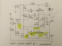
I just thought of a place to plug in my Cree MOSFET kludge circuit to see how it sounds. One of my favorite little Pass designs is the ACA amp camp amp. Per Pico's suggestion to just plug it into a mu follower circuit, and since I have a stereo pair on the shelf, I thought I would give it a go. The curves I ran for the Schade SiCfet network showed me that to get the bias of the SiCfet up to 1.1 Amp at a drop of ten volts, I need a VGS of 6 volts. The 2SK170 I used in the build had an IDSS of about 5mA, which will only develop a max of 5 volts across the 1K R9, I upped it to 1K5. The Schade network is made from a new R6 value of 10K, and added resistor from Q1's Drain to Gate of 100K. Q1 is the Cree and Q2 is the original IRFP240. Since the input capacitance is much lower than the IRFP part I'm hoping that frequency response won't suffer too much from the R6 increase.
What do you guys think? Am I thinking right or am I missing something?
What do you guys think? Am I thinking right or am I missing something?
Attachments
Last edited:
I finally took the plunge and ordered four of the new C3M SiC FETs in TO-247. Added $40 to my Mouser bill. 😱 Not as bad as some NOS tubes, though.
They should arrive tomorrow, but it will be some time before I get them built into a circuit. I am planning to try them in the F6. Sadly, I don't have any fancy test equipment to use for posting curve traces and such.
They should arrive tomorrow, but it will be some time before I get them built into a circuit. I am planning to try them in the F6. Sadly, I don't have any fancy test equipment to use for posting curve traces and such.
I finally took the plunge and ordered four of the new C3M SiC FETs in TO-247. Added $40 to my Mouser bill. 😱 Not as bad as some NOS tubes, though.
They should arrive tomorrow, but it will be some time before I get them built into a circuit. I am planning to try them in the F6. Sadly, I don't have any fancy test equipment to use for posting curve traces and such.
Needtubes
No need to be apologetic. We all use what we have. My stuff is far from fancy - the curve tracer was a kit I built forty years ago. Besides my scope, the best investment I ever made in test equipment. My scope is Almost as old - a Tektronix 465 B. You can buy these for really good prices used on the net.
Believe it or not I have used the tracer and learned more with it being part of the DIYAudio community than in all the years before. You will love your amp when you get it built.
Why are R1 & R2 different value than R3 & R4? Makes no sense...
Why are the tops of P1 and your 100K Schade not referenced
to the node closest to the output, between R1 and R3?
There should be some small resistance between C2+ and the
node shared by R5 + collector Q3.
Given feedback through P1, hasn't Schade already been achieved?
This new network is redundant, not that a little local feedback is
a bad thing...
Last edited:
Kenpeter,Why are R1 & R2 different value than R3 & R4? Makes no sense...
Why are the tops of P1 and your 100K Schade not referenced
to the node closest to the output, between R1 and R3?
There should be some small resistance between C2+ and the
node shared by R5 + collector Q3.
Given feedback through P1, hasn't Schade already been achieved?
This new network is redundant, not that a little local feedback is
a bad thing...
Thank you for your comments and observations. The goal of my little experiment was to drop my Schade network as a "black box" into a proven design to see how it would perform (or if it would ). Part of the goal was to change the least part of the design possible to allow side by side comparison of the modified and unmodified circuits. The things I did in pursuit of this goal may not make any sense. I built the circuit as drawn and it biased up normally, but when I ran audio through it there was distortion on peaks. I will put it back on the bench and see if I can discover why. Your clues will help me think about what might make it function properly. I always learn more from my mistakes than successes.
Mike your approach is pretty cool.
One of the things you might want to think about is the interaction between the existing bias network and the bias introduced by the schade network resistors.
I'm certain you'll get there in the end but meantime before changing anything else, why not put a reasonably sized capacitor in series with the 100k resistor and see where that takes you.
Many small steps are going to take you a very long way - Good luck !
kasey197,
Thank you for your post. That will be super easy to try. I see what you are saying about interaction between bias networks. The cap will restrict the interaction to AC and block DC. I have some nice Silmic II's that I can add and we'll see what happens. One thought I had is that the transconductance of the SiCfet I used is much less than the IRFP240 it replaces. I have read that the lower device of a mu follower should have higher transconductance than the top. In my case the reverse is true.
Thank you for your post. That will be super easy to try. I see what you are saying about interaction between bias networks. The cap will restrict the interaction to AC and block DC. I have some nice Silmic II's that I can add and we'll see what happens. One thought I had is that the transconductance of the SiCfet I used is much less than the IRFP240 it replaces. I have read that the lower device of a mu follower should have higher transconductance than the top. In my case the reverse is true.
Given feedback through P1, hasn't Schade already been achieved?
This new network is redundant, not that a little local feedback is
a bad thing...
SICFET in mikegranger's schematic was Schaded to generate a Pseudo-SIT. This resultant new triode-amp is further "Schaded" via the original pathway of the parent amp per your post above. Aside from his reported distortion on peaks of this "doubly Schaded" amp, did this redundancy [double feedback] add a discernible sonic value beyond that granted by the parent amp? Does one of the feedback pathways now default to a normal Black feedback, and thus is a harmless good practice?
kasey197,
One thought I had is that the transconductance of the SiCfet I used is much less than the IRFP240 it replaces. I have read that the lower device of a mu follower should have higher transconductance than the top. In my case the reverse is true.
I must have misread your older post. So, you have the Cree's only in the bottom of the mu-follower with IRFP240 on top? Sounds like that is the way it should be in a mu-follower type circuit where a more potent "cathode follower" is stacked on top of a weaker tube.
nothing wrong with IRFP in place of Mu
in fact , I'm pretty sure that part with greater xconductance is of benefit there
in fact , I'm pretty sure that part with greater xconductance is of benefit there
I must have misread your older post. So, you have the Cree's only in the bottom of the mu-follower with IRFP240 on top? Sounds like that is the way it should be in a mu-follower type circuit where a more potent "cathode follower" is stacked on top of a weaker tube.
I've been trying to understand the mu follower function for a long time. I still have a long way to go to really know how it functions. I first read about it in the old National Semiconductor Audio Applications Databook (I still have my original copy) in the chapter titled Fet Audio Applications (AN 32) .
On page 6, there is a circuit for a very high gain FET mu amplifier. In the brief description they talk about how the upper Fet needs to have less transconductance than the bottom. In fact the part numbers are different denoting the intentional mismatch between the devices. I was thinking of that circuit when I wrote my earlier post.
If you want to take a look at the book, it's online in the TI library. Lots of really cool old school designs there. Some look very familiar....
Attachments

Last edited:
Well it seems I had that backwards.... The higher transconductance Device ( 2n3684) is on top. I need to go back and study some more now that I've realized I was looking at it the wrong way.
This is my very basic understanding.I've been trying to understand the mu follower function for a long time. I still have a long way to go to really know how it functions..
The output at the drain of Q1 (common source) drives the speaker load and the gate of Q2 (common drain) which adds extra current gain but no voltage gain to the original signal at the load. So amp is able to deliver twice bias current into load.
It's definiitely my favourite amp topology, that doesn't mean it is the best amp, I just love the way it functions.
I can give you a more raw form of the circuit to play more directly with the schade effect similar to the above circuit.
Last edited:
Thanks Pico. That would be great. I'm going to put a sine wave through my experiment this evening and take a look with the o'scope. Maybe I can see what is happening.
Voltage at the source of the follower SICFET moves identically to the drain
of the Schaded SICFET, with just enough offset to forward bias the base of
the BJT and let the BJT prevent the follower's gate bias cap further charging.
The load is attached to a resistive voltage divider between output devices.
These measure the class A current total and present it to the BJT for bias
control.
You can get a lower output impedance and higher Mu accuracy by loading
closer to the top of the voltage divider. But reality this does not drive low
impedance loads as well as loading at the center. If it can't swing the full
required current in both push and pull, it matters not what was impedance.
Center best shares the load current swing between the two devices.
This is why I do not agree as-drawn, with load for some reason not center.
Maybe for a 32ohm headphone this makes sense, but not for speakers...
- Home
- Amplifiers
- Pass Labs
- new SiC JFETs?