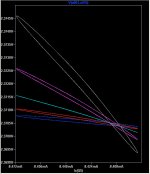
So here's a stepped plot of the bias spread as a function of VAS current. From top to bottom 112R, 56R, 28R, 14R, 7R.

Cordell and Hawksford are trying to make this flat. But flat doesn't seem to be the only issue -- some values cause more time variance. I presume that's between signal rise and signal fall and is due to the fact that the VAS transistor can switch on much faster than off?
28R is indeed the optimal value for flattening the time variance. The width of the ovals (and the optimal R value) are also highly dependant on the Cdom value (presumably because it's the Cob that most affects the turn-off lag?).
So is the ovality indeed separation in rise and fall? And if so, can we conclude that minimising bias spread as a function of rise/fall is more important than minimising it as a function of VAS current?
Attachments
NAP140 from post 106
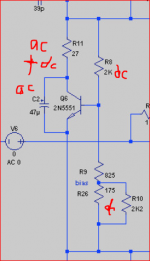
What I see in your circuit is a low shunt path to bypass a.c. around Q6 so the ac signal does not influence the dc connection to Q6 base. The a.c. current through R11 via C2 will ride on the d.c. current passed from Q6 collector and drop low level of d.c. voltage. In effect the voltages are being mixed within the resistor so the two signal sources are summed before arriving at the driver transistor base.
Referring to post 1 the original value for C2 equivalent part number was 22uF and this was increased to 220uF which reportedly resulted in a subjective change in the quality of the low end response. The depth of the bass was perceived to increase but this thought to be less tight in character.
Later when C2 was removed the amplifier became unstable. R11 then formed a collector load and this should have been replaced by a wire link.
Attachments
Based on mjona's info I plotted the rate of change of the voltage spread across the bias spreader transistor. The outside two traces are the closest E24 values (24 & 27), while the inside two are E48 values (24.9 & 26.1).

These would argue for a 25ohm optimal, with 24 a slightly better choice than 27 out of the E24 series. The plots diverge fairly quickly after that; 27 (while not being dead-on optimal) is still better than 22 or 33.
Wondering if these were two different ways of measuring the same phenomenon I ran the V=f(I) plots again with the values from above. They do not agree: 28ohms is still the optimal for minimising the time-variance in the the V=f(I) plots.
So, was 27 chosen as a compromise between these two optimisations? Or was Vereker going for one or the other and getting it dead-on just doesn't matter that much?
Attachments
Linsley-Hood used 27R in his 75W amplifier published in Hi-Fi News and Record Review in November 1972. He shared the circuit with some other people to test the reliability of the design prior to publication of the article.
It may be coincidence that the value of 27R happens to be a multiple of 0.27R the value of the power transistor emitter resistors in Hood's original design which has the Vbe transistor mounted on the heat sink.
Naim use 27R with 0.22R power transistor emitters. The vbe transistor is mounted on the pcb and the output stage current is a lot less than in Linsley-Hood's design.
Self's designs typically use 0.1R emitter resistors and his choice of resistor in the Blameless amplifier was 16R. He puts his vbe transistor on the power transistor case. I have not looked to see what standing current for the output stage is.
The slope is the resistance of the circuit. Eyeballing your graph I estimate the 28R line to be about 16 ohms. You can never make this flat because that would be zero resistance.Cordell and Hawksford are trying to make this flat. But flat doesn't seem to be the only issue --
Last edited:
The slope is the resistance of the circuit....
Half of that resistance (Rcb) is dynamic and in the opposite direction of a "normal" resistor, no? So you can make it flat by making Rcb track more-or-less to R.
The wrinkle of course being that then I need to measure it from where Hawksford and Cordell would drive the upper driver from, rather than from where JV did. But when I do that, it goes flat at 16ohms, which still doesn't meet their predictions. 😉
I think I might smash a DIP socket with machined pins and put a couple of the pins in where that resistor goes. I'm curious if you can hear any difference between, say, 10 and 68ohms....
What circuit nodes does you graph in post #121 measure? Is it across the whole vbe circuit or just the transistor CE or somewhere else?
Ok, that's what I thought. The idea is not to make the resistance zero between these nodes. That wouldn't really add much value. There is a different idea at play. 😉#121 is the whole Vbe circuit (bottom of VAS transistor to bottom of Vbe transistor).
Good idea to listen for a difference.
Coincidence.It may be coincidence that the value of 27R happens to be a multiple of 0.27R the value of the power transistor emitter resistors in Hood's original design which has the Vbe transistor mounted on the heat sink.
From a different perspective
I have attached some graphs showing the relationship between base emitter voltage and collector current. The first of these shows the relationships assuming the vertical and horizontal scales are uniform.
In the second image for BC547 the vertical scale has some compressed spacing of the divisions. This is convenient for using a straight line plot allowing a ruler to be placed on the graph to vector vertical and horizontal intersects and read off the values on the corresponding scales.
In the third image it is the horizontal scale that has some compressed spacing of the divisions for the same reasoning - but in so doing this masks some curvatures indicated by the first image.
Looking at the second and third graphs it is still clear that an increase in temperature will increase the collector current quite markedly since the slope in the first graph is steep.
It is common to use gm as a measure of the ratio of vbe to Ic. This is equal to Ic(q/kT) where q is the charge on the electron, k is Bolzmann's constant and T the Elephant in the room since this depends on the absolute temperature of transistor junction.
In turn this would depend on the ambient temperature in the room, the amount of output stage current under quiescent and dynamic operation the size of the heat sinks etc.
gm is measured in Siemens (S) 1 volt in for 1 ampere of collector current - scaled down to suit the graphs with m.V. and m.A.
The gm measure would then be in mS. For a typical small signal transistor with the junction temperature at 25 degrees C, a practical value of mS is in the vicinity of 40mS (m.A./V) per m.A. from 1m.A. and upward as applied in a Vbe situation.
If there is an increase in the junction temperature the gm slope will increase raising the possibility of the bias current being increased to the point where Vbe is reduced and cross-over distortion becomes significant.
gm has an opposite relationship with resistor - ignoring component % tolerance 1A input voltage across 1 Ohm dropping 1 Volt is a linear result.
The amount of Vbe current will be limited by what is available CCS probably about 7-8 m.a. total in the Naim circuit.
If part of the voltage drop over the critical range of a Vbe can be made linear by a low value resistor load in the collector connection you would put that knowledge to use.
While the images give some information, in the era of the 70's when Julian Vereker was developing this amplifier a transistor curve tracer would have been a handy laboratory asset. It is on record that Vereker had one and did all his test measurements himself.
Ok, that's what I thought. The idea is not to make the resistance zero between these nodes. That wouldn't really add much value. There is a different idea at play. 😉
Good idea to listen for a difference.
I have attached some graphs showing the relationship between base emitter voltage and collector current. The first of these shows the relationships assuming the vertical and horizontal scales are uniform.
In the second image for BC547 the vertical scale has some compressed spacing of the divisions. This is convenient for using a straight line plot allowing a ruler to be placed on the graph to vector vertical and horizontal intersects and read off the values on the corresponding scales.
In the third image it is the horizontal scale that has some compressed spacing of the divisions for the same reasoning - but in so doing this masks some curvatures indicated by the first image.
Looking at the second and third graphs it is still clear that an increase in temperature will increase the collector current quite markedly since the slope in the first graph is steep.
It is common to use gm as a measure of the ratio of vbe to Ic. This is equal to Ic(q/kT) where q is the charge on the electron, k is Bolzmann's constant and T the Elephant in the room since this depends on the absolute temperature of transistor junction.
In turn this would depend on the ambient temperature in the room, the amount of output stage current under quiescent and dynamic operation the size of the heat sinks etc.
gm is measured in Siemens (S) 1 volt in for 1 ampere of collector current - scaled down to suit the graphs with m.V. and m.A.
The gm measure would then be in mS. For a typical small signal transistor with the junction temperature at 25 degrees C, a practical value of mS is in the vicinity of 40mS (m.A./V) per m.A. from 1m.A. and upward as applied in a Vbe situation.
If there is an increase in the junction temperature the gm slope will increase raising the possibility of the bias current being increased to the point where Vbe is reduced and cross-over distortion becomes significant.
gm has an opposite relationship with resistor - ignoring component % tolerance 1A input voltage across 1 Ohm dropping 1 Volt is a linear result.
The amount of Vbe current will be limited by what is available CCS probably about 7-8 m.a. total in the Naim circuit.
If part of the voltage drop over the critical range of a Vbe can be made linear by a low value resistor load in the collector connection you would put that knowledge to use.
While the images give some information, in the era of the 70's when Julian Vereker was developing this amplifier a transistor curve tracer would have been a handy laboratory asset. It is on record that Vereker had one and did all his test measurements himself.
7R does a better job than 28R at minimising the delta due to temp (measured via V at the bias spreader and at the driver bases, and via I at the output stage source resistors). (I measured at 25ºC, 40ºC and 60ºC.)
Neither one does all that much, though. T is indeed the elephant in the room.
So I'm still at a loss....
Neither one does all that much, though. T is indeed the elephant in the room.
So I'm still at a loss....
7R does a better job than 28R at minimising the delta due to temp (measured via V at the bias spreader and at the driver bases, and via I at the output stage source resistors). (I measured at 25ºC, 40ºC and 60ºC.)
Neither one does all that much, though. T is indeed the elephant in the room.
So I'm still at a loss....
My advice is to stick with 27R.
T in the formula I gave you as "absolute" relates to junction temperature on the Kelvin scale.
Accordingly 25 degrees C ambient is 298.15 K and 40 C is 313.15 K.
The junction temperature of the Vbe transistor will depend on where located. It would be hotter on a heat-sink or glued to an output transistor.
In a Naim amp it is located on the pcb and the enclosure is so designed to keep the heat inside at a steady level aided while being powered by the mains at all times.
To work like this the Vbe would have to be highly attuned for minimal variation - low standing current in the output stage. I have a Nait 5i - I bought it new and have never been tempted to look inside the case.
There is a slight difference between TA ambient temperature and T junction temperature.
A point to note is T in the gm formula is a divisor so increasing the junction temperature of the Vbe transistor will change the gm at junction temperature of 25 C (298.15K) where slope is 40m.S. or 40 m.A./Volt.
The slope will become steeper. You have to work around that problem and I think there are enough clues in the material on this thread to serve as leads for you to follow up on.
I let LTSpice do the math for me. It takes temps in ºC, and I'm pretty sure uses them for junction temps rather than ambient.
I let LTSpice do the math for me. It takes temps in ºC, and I'm pretty sure uses them for junction temps rather than ambient.
Not as standard but you can use the .step command there are tutorials you can look at to show how - like the one at this link YouTube The tutor does go on a bit.
That's not it.If part of the voltage drop over the critical range of a Vbe can be made linear by a low value resistor load in the collector connection you would put that knowledge to use.
Looking at it in the frequency domain something between 14 and 18ohms produces the flattest bias spread over the audio range.
But it has no effect on the output, so this seems like a red herring....
How about a hint, Brian?
But it has no effect on the output, so this seems like a red herring....
How about a hint, Brian?
Looking at it in the frequency domain something between 14 and 18ohms produces the flattest bias spread over the audio range.
But it has no effect on the output, so this seems like a red herring....
How about a hint, Brian?
Total silence.
R11 in your Vbe passes separate currents merged firstly between the lower divider resistor and the emitter- base current.
Subsequently the collector current is added into that mix.
The total mix will pass through R11 which happens to be in the position of loading the collector of the Vbe.
The a.c. signal is diverted around the collector to emitter junction so you are just considering d.c. around a common emitter structure albeit small in scale.
This type of circuit inverts the signal so the voltage drop across R11 will register as negative in phase. The divider network provides a suitable nfb connection from the collector to the base.
- Status
- Not open for further replies.
- Home
- Amplifiers
- Solid State
- Modified Naim NAP140 Schematic