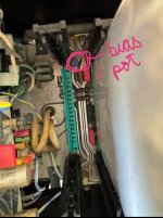
It's a bit more complicated.Adjust this pot first. Connect a voltmeter to the output terminal. The DC offset should respond to this pot adjustment. If you can’t get it near to zero DC volt, then you will need to adjust the other pot sandwiched between the two boards. You need to be careful adjusting the second pot. You will require an insulated long screwdriver for this. See my photo to locate the second pot.
when you remove the power transistors from the heatsink, you can still reuse the mica sheet if they are not damaged. It’s easy to wipe off the old heat grease and get further cleaning with alcohol solvent. Reapply heat compound and mount back. Mica sheet does not degrade over time and can be reused.
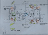
Look at the diagram below.
The 20.6 has a separate buffer amp on the upper piggyback board.
The pot that KweeSong is pointing to is to adjust the offset of this buffer amp, but as you can see the 10uF below the main amp will only just temporarily react to this adjustment and then go back to its own offset.
When adjusting this pot look at junction P502, you can see this point on KweeSongs image on the lower corner at the right just above the big blue cap of the lower board.
To adjust the offset of the main amp, you will have to adjust another pot, see below.
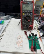
And the bias current has to be set at 2.8Amp with the pot on the motherboard as below and measured on either R22 or R23
A final point of adjustment are both +/- regulated supply voltages going to the main amp. When not equal to within 100mV, a soft start circuit on the piggyback board will prevent the amp from working properly.
This will have to be adjusted on the other RP3 board.
Hans

Cheers, Hans.I'm just a normal person who was angry to be left in the dark by ML. All the local ML dealer offered was to replace my teflon boards by Arlon boards for a ridiculous price of 4000,- Euro per per board, so in total 8000,- Euro., which I did not accept.
Lot's of time went into the reverse engineering, since no circuit diagram in any form was available at that time.
But to be fair I'm a MsCEE, so it was possible for me to unravel all details.
Hans
I am so lucky to have Mr. Lim and Hans, two experts and professionals who taught me more about the adjustments! Really impressed and very grateful to the gentlemen!
I will not post the part where I tested the other modules independently on the bench with jigs I designed. If anybody is interested just let me know.
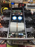
I will attached a few pictures here. This process took more than a week to complete.
Photo show jig and test set up to test the output current biasing function
"I will not post the part where I tested the other modules independently on the bench with jigs I designed. If anybody is interested just let me know."
Hello Mr. Lim,
I am very interested in the testing of various modules. When you have time, please share the pictures as well as how your jig and tests were done. The readers will benefit much by learning this. Thank you very much!
As requested, let me described how I tested the various module independently.
First the voltage regulated voltage module. The function is located actually on two separate modules.
1. The reference voltage and the driver circuit is located on RP3 board
2. The output transistors are located on two separate heatsink modules. Marked as NRP and PRP, negative regulator and positive regulator respectively.
Attachments

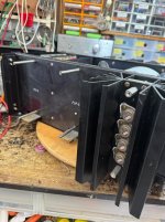
On the left is the PRP module, the right side is NRP.
The other four modules are removed, namely PBP, NBP (bias modules) and PDP, NDP (drive modules) to test the voltage regulators.
When I tried to test the power supply would not turn on. Took me a while to figure out. I had to study closely the protection circuit.
I eventually found out that in order for the system to power up, all the six modules must be installed. Reason being that there were four thermal switches that were located in the other four modules. Without installing them the thermal switches will appear as open (over temp) and the amp will not power up.
So I installed four jumpers to trick the protection circuit that the thermal switches are operating.
Attachments
Sorry I remembered wrong. Thermal switches on the NDP and PDP modules only. There is on more thermal switch somewhere within the chassis. That one is connected so no issue.
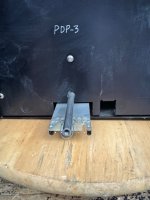
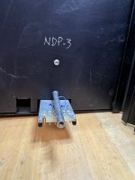
With the jumpers installed I could turn on the amp and measure the regulated voltage at the edge connector pins located at the PDP and NDP sides.
I was able to confirm that the voltage regulators drivers on the RP3 board are working including the NRP and PRP output modules.
Stay tuned. I will describe how I tested the drivers and the bias section of the AP5 board.
I was able to confirm that the voltage regulators drivers on the RP3 board are working including the NRP and PRP output modules.
Stay tuned. I will describe how I tested the drivers and the bias section of the AP5 board.
Cheers, Mr. Lim. What a wonderful continuation of the post! Waiting patiently for more.See photo for location of jumpers
This block diagram is very important and useful to understand how the various modules of the amplifiers are connected. Pay attention to the pin # notation. I wish o found this diagram sooner. I was searching for more information and found this which was for the ML2 but basically similar to the ML20.6.
Attachments
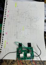
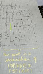
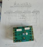
I redrew the schematic to help me understand how the modules are connected so I could figure out how the idle current biasing works.
The schematic represents a combination of the various modules connected. To test the bias function the AP5 board, NBP,PBP, NDP, PDP and some other components on the chassis motherboard needs to be connected.
If these modules were assembled I won’t be able to probe and measure any voltages.
See the photo of the bias adjustment pot. It is way down on the chassis motherboard and not easily accessible once RP3 and AP5 are inverted.
So to test that AP5 is working, I decided to make a test jig to simulate the rest of the circuit to be connected to AP5
Attachments

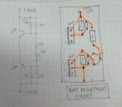
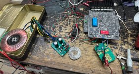
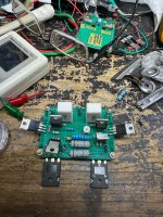
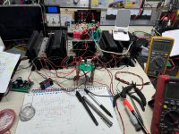
This is the test jig for the bias adjustment circuit. Note that on the system connection, one transistor is on the PBP module and the other is on the NBP module and the pot is on the motherboard. I checked that the jig is working as intended before connecting to AP5
Attachments
I had to hooked up a high voltage (+/- 55V) DC supply to test this. My bench power supply does not go up this high.
With that I was able to test the AP5 module. I was able to adjust the bias voltage.
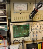
I connected a sine wave to the input and checked if the AP5 input and driver stage are working. Measured the output and got a very distorted almost square wave output.
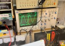
Figured later that I did not make the feedback connection. Once connected, the AP5 driver output showed a nice sine wave.
With that I concluded that the AP5 board was working
With that I was able to test the AP5 module. I was able to adjust the bias voltage.
I connected a sine wave to the input and checked if the AP5 input and driver stage are working. Measured the output and got a very distorted almost square wave output.
Figured later that I did not make the feedback connection. Once connected, the AP5 driver output showed a nice sine wave.
With that I concluded that the AP5 board was working
Attachments
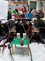
Next to connected the four NBP PBP NDP PDP modules to AP5 to test. For that I need another test jig, a simpler one.
This jig simulates the components which are on the motherboard.
For this test, the system block diagram is very helpful. I had to figure out how each module is connected to the next.
You can see that on the drawing of the connection diagram I made.
This jig simulates the components which are on the motherboard.
For this test, the system block diagram is very helpful. I had to figure out how each module is connected to the next.
You can see that on the drawing of the connection diagram I made.
Attachments

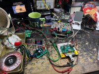
Later I added the rest of the components to simulate both NBP and PBP to the test jig.
With that I was able to power up the AP5 with the test jig with the output transistors on a small heat sink. I biased the output stage to a lower power rail (+/-10V) to limit the power dissipation.
I was able to send a music source to the boards and play music through a speaker.
So far so good.
With that I was able to power up the AP5 with the test jig with the output transistors on a small heat sink. I biased the output stage to a lower power rail (+/-10V) to limit the power dissipation.
I was able to send a music source to the boards and play music through a speaker.
So far so good.
Attachments
Next was to connect the actual modules to The AP5. The small test jig with the bias pot was still necessary.
For that the system interconnection is very important. See the diagram in the attached photo.
With all these careful and step by step approach it was less anxious to finally connect all the modules together and power up.
The modules powered up without a hitch. Bias current was at 1A and was able to play music.
Attachments
After this step I reassemble the amplifier and the amp was able to power up but play for a period of time and protection was triggered again.
The rest of the story starts above posted earlier.
This conclude the whole story of of this repair.
In summary:
1. The system interconnection is very important to understand this amplifier. Any module remove will stop the amp from powering up.
2. One cannot probe and measure any voltages once all modules are connected.
3. To do so would require an edge connector extender so both AP5 and RP3 can be raised above the chassis to probe. I did not have access to this jig and too difficult to build.
4. Once module is removed it does not work on its own unless a test jig is build to test its function.
5. This amplifier is very elaborate and an in depth knowledge is necessary even with the schematics on hand. Without them it will be even more difficult. I had to study and learn as I progressed step by step.
6. It was very satisfying to eventually fixed and get the amplifier running.
Hope you enjoy the entire journey and have a chance to learn from my experience.
😊
- Home
- Amplifiers
- Solid State
- Mark Levinson No. 20.6 Repair