All of the current AGC elements (FET or analog multiplier) have full bandwidth so any stuff on the control input comes through the system. In the jfet case I encountered the problem with the KH4400. I can null the 2nd from the jfet with the distortion trim. But the harmonic spectrum on the gate of the JFET is also on the main output (attenuated a lot but still there). The higher order harmonics are attenuated but not gone. I was speculating about taking an inversion of the signal going to the gate and adding it to cancel the harmonics. Not sure that would work however.
I'm not sure if the linearity of the AGC element is a problem until this issue can be resolved.
Whether the linearity of the agc element is the dominant source of distortion or not will depend on the oscillator design and the component values. It would be a shame, for example, for someone to go to the trouble of implementing an S/H level detector only to discover that the dominant source of distortion was the agc element. That's why I mentioned the two experiments above that can be carried out to separate out these two sources of distortion. In trying to improve a design, it is very important to attack the dominant source of distortion first.
Cheers,
Bob
...Here is the low parts count 4 phase solution I used. It takes advantage of the open collector LM339 which will behave as an amplifier with pull down but no pull up. No diodes or diode drops to deal with. Trimming to get 4 peaks at exactly the same level would be an issue. Speed up tricks etc. to be added. Still not as good as a sample and hold-track and hold but fewer parts and no fast edges.
This is a "4-phase" absolute value detector I did to emulate the SSL Bus Compressor "greater of four" peak detector.
The first version I tried used a diode pre-distorter driving 2X THAT1646s to provide anti-polarity outputs feeding un-biased diodes. The pre-distorter overcomes diode Vf. I chose the 1646 because it has precision internal resistors to provide signal inversion and has high-current outputs. The circuit picks the greatest of four peaks in L and R which in the case of an oscillator could be the sin and cosine inputs.
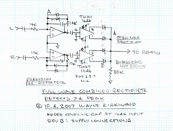
Greater of Four Absolute Value Detector Using A Diode Pre-Distorter.
I found a later version which pre-biases the rectifier using the THAT1646 Sense inputs. The sense inputs provide a "common mode" output voltage to bias the rectifier diodes. The THAT1646 differential input is fed with signal. This pre-bias is similar to Bob's approach with diodes substituted for the transistors. Unlike the first example this one is "class-A" with no op amps running open loop. I tested the first one. I flat-out don't remember if I tested this example. YMMV.
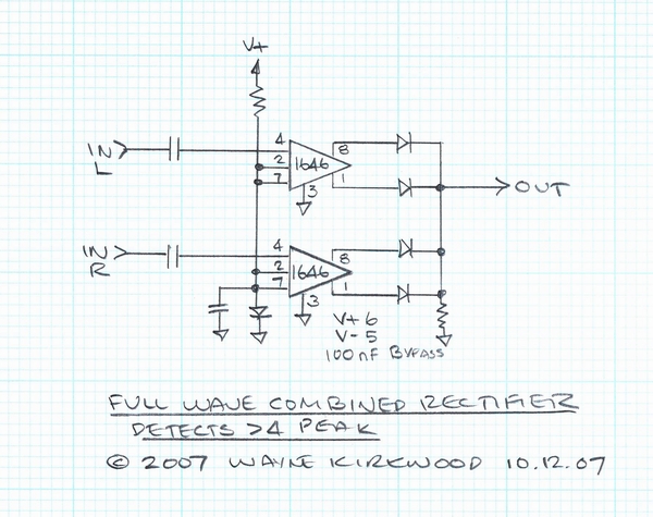
Greater of Four Absolute Value Detector Using Diode Pre-Bias.
I pulled out diodes to make it half-wave so it could be visualized. One channel has a higher level at high frequency; the other channel about -6dB and lower frequency. (So I know that I built one of these LOL.) The in-phase and quadrature signals in an oscillator would be identical level so this doesn't illustrate how it would look as a 4-phase rectifier.
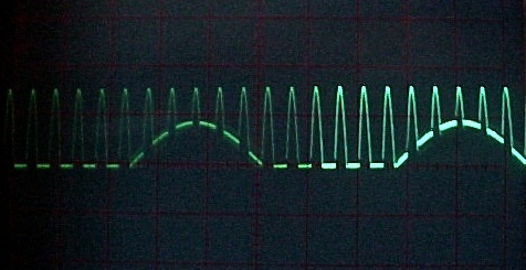
"Greater of two" peak detector.
The 1646 makes things considerably simpler. You could certainly do the same thing with op amps and precision resistors.
The 1646 output offset with OutSmarts turned off is typically around 5 mV. In an oscillator or compressor/limiter application low-level performance isn't a great concern. The symmetry should be quite good.
The offset and diode thermals are only important where absolute AC accuracy is important. Getting that right brings a lot more circuitry to the task. The Fluke 510 below has more circuitry devoted to level sensing than to oscillation. I did some tweaks and got the distortions down to the -120 dB level for the harmonics on this.
Attachments
The offset and diode thermals are only important where absolute AC accuracy is important.
True. The Fluke looks to sample the peak of the log of the absolute value of Ein.
As to offset from Vf, Smith didn't even deal with that connecting the rectifier diodes directly to the outputs through 100KΩ resistors. Since the rectifier should be buffered for isolation it's not a bad idea to pre-bias them since it only takes a diode and resistor and it improves linearity below a few volts or so.
Thermal differences between diodes will affect the symmetry of the rectifier output. Placing them close to each other reduces that enough IMHO for this oscillator.
Two questions I'd like to ask:
Viktor: Your circuit takes Vds/2 and injects it back into the gate via the op amp driver to reduce FET distortion. Is additional FET distortion cancelled by the unique signature of half-wave ripple? Did half-wave provide an advantage over full-wave for any particular reason?
Bob: Regarding a SV oscillator with sin cosine outputs. You mentioned that the "four phase" (sin/cos full-wave rectified) could be made "8 phase" by combining the sin cosine outputs. If the sin cos outputs were "summed" and "differenced" wouldn't this provide two additional outputs with 45° offsets?
If so, it would be very simple to implement and without much circuitry move the ripple frequency farther out-of-band.
For a fixed-frequency Wien oscillator not having a 90° output it seems like one could be derived with an allpass filter to build a "four phase" rectifier and with addition/subtraction stages extended to eight phases.
Four and eight phase is not as over-the-top as I first thought.
Two questions I'd like to ask:
Viktor: Your circuit takes Vds/2 and injects it back into the gate via the op amp driver to reduce FET distortion. Is additional FET distortion cancelled by the unique signature of half-wave ripple? Did half-wave provide an advantage over full-wave for any particular reason?
Bob: Regarding a SV oscillator with sin cosine outputs. You mentioned that the "four phase" (sin/cos full-wave rectified) could be made "8 phase" by combining the sin cosine outputs. If the sin cos outputs were "summed" and "differenced" wouldn't this provide two additional outputs with 45° offsets?
If so, it would be very simple to implement and without much circuitry move the ripple frequency farther out-of-band.
For a fixed-frequency Wien oscillator not having a 90° output it seems like one could be derived with an allpass filter to build a "four phase" rectifier and with addition/subtraction stages extended to eight phases.
Four and eight phase is not as over-the-top as I first thought.
Yes, the additional 4 phases for the 8-phase detector are obtained very simply by addition/subtraction of the positive and negative phases of the sine and cosine signals. In principle, it only takes 4 op amps to do this.
Cheers,
Bob
Thanks Bob.
Going back to my question to Viktor.
Halfwave rectification will produce a ripple component at the fundamental frequency in the detector. When the oscillator output is multiplied by the fundamental ripple component we get added 2f in the output.
Is the deliberate introduction of 2f from detector ripple into the output used to cancel the residual even-order distortion of the FET? This was the "magic" I spoke of earlier.
No.Is additional FET distortion cancelled by the unique signature of half-wave ripple?
No.Did half-wave provide an advantage over full-wave for any particular reason?
You can get little advantage, when the small double frequency ripple (as full wave detector can produce) in the properly phase is injected to the AGC FET gate (and also Vds/2 of course).
The oscillator was designed with the minimalism concept for the best performance/cost ratio. The small part of the oscillator signal across the FET (0.5%) and the big time constant is the key to get the signal harmonics down to -150dB and lower level.
Victor.
Last edited:
The oscillator was designed with the minimalism concept for the best performance/cost ratio.
Victor.
And you have achieved that superbly and elegantly.
Thank you for the insights.
I don't get this logic. While its true that a FWR injects second harmonic, it also injects much higher harmonics as well. A half-wave rectifier injects everything from fundamental on up. The higher harmonic frequencies injected by a given rectifier will receive more attenuation by the control loop filter than the lower harmonics, for a given amount of loop stability and settling quality.
A FWR has p-p ripple equal to the peak value of the signal. A 4-phase rectifier has p-p ripple only on the order of 30% of the peak value of the signal, and its lowest ripple frequency (in the ideal case) is 4X the fundamental, as compared to 2X the fundamental in a FWR. This means that in a first-order control loop filter, its harmonics will see 6dB more attenuation than those from a FWR.
Cheers,
Bob
I was not thinking of all the garbage from the detector.
I was thinking of the filtered wave form modulating the resistor/LED combination and thus the oscillator circuit.
the half wave modulation would equal F and the full wave modulation would equal 2F.
thus the oscillator would be modulated at 2F for a full wave detector.
One way through this if amplitude saccuracy is not a major issue would be an incandescent lamp coupled to an appropriate photocell. The lamp will integrate the energy from the source in a proper RMS way. The photocells aren't too fast either. Or you could use a PV cell driving a JFET. Response time is slow so not for applications that need fast response or precise levels.
...In principle, it only takes 4 op amps to do this...
Plus the rectification circuitry presumably?
The "sum of two squares" approach could be done with a LM13700, one IC and just over $1.
I am interested in this for a tunable oscillator but it starts to look pretty reasonable even for a fixed frequency unit.
Have you considered this approach?
One way...would be an incandescent lamp...
An oscillator based around an incandescent lamp control... I could swear I've seen that before😉
Best wishes
David
Not much response on "sum of squares" level detector, hopefully more interest in the next circuit block.
Bob's oscillator has Q1 controlled IC3 for active feedback but that doesn't look necessary.
It could be simplified to have the FET in the feedback path to control the loop gain directly.
I favor the simpler technique but perhaps I have missed some point, anyone see a problem?
David
Bob's oscillator has Q1 controlled IC3 for active feedback but that doesn't look necessary.
It could be simplified to have the FET in the feedback path to control the loop gain directly.
I favor the simpler technique but perhaps I have missed some point, anyone see a problem?
David
Not much response on "sum of squares" level detector, hopefully more interest in the next circuit block.
Bob's oscillator has Q1 controlled IC3 for active feedback but that doesn't look necessary.
It could be simplified to have the FET in the feedback path to control the loop gain directly.
I favor the simpler technique but perhaps I have missed some point, anyone see a problem?
David
Hi David,
Its been a long time since I designed it, but the JFET arrangement with IC3 was, if I recall, there to enable the application of both the dc control signal and the 50% drain signal feedback without resort to doing some sort of ac coupling of the feedback signal. Again, my recollection of all of the details is a bit fuzzy, but I do remember giving it a lot of thought. In some of the simpler JFET agc element arrangements, I think the control signal was delivered to the gate through a high-value resistor, and the feedback signal was delivered to the gate from a drain-source voltage divider via a coupling capacitor. This arrangement added a pole in the control loop, and I wanted to avoid that.
Having IC3 there also gave me gain, so that I could have a small signal across the JFET while still having a larger final agc signal that could be injected into the SV loop through a relatively high resistance. I think that injecting the correction signal into the SV loop through a high-value resistor may also have some noise advantages with respect to the thermal noise of the injection resistor.
I think the arrangement also acted as a type of bridge, so that if no agc gain trim of the SV loop was necessary, no signal would be injected into the SV loop through the high-value injection resistor. This of course does not mean that under these conditions there is no signal across the JFET.
I suppose with a little further thought and circuitry, one could use a dual-matched JFET with one JFET acting as a replica on one side of the bridge to get some cancellation of JFET distortion in the balanced condition where little or no correction signal is injected into the loop. Just thinking out loud here, and it might not be worth the trouble.
The cost of the whole IC3 arrangement was of course negligible.
Cheers,
Bob
Or you could use a PV cell driving a JFET.
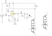
Anyone ever try this? J1 and J2 form a FET with center tapped channel eliminating the need for the resistors to split the drain source voltage. The drive is totally galvanically isolated too. The two FET's and R1 just a short, no PV is used as a nice bi-directional current limiter on amplifier inputs. It looks like a 50-100 Ohm resistor for a FET like an SK170 but limits current to Idss even with no power applied, aerospace loved it.
I think it would make a nice non-clipping fuzz pedal too.
Attachments

Last edited:
Anyone ever try this? J1 and J2 form a FET with center tapped channel eliminating the need for the resistors to split the drain source voltage. The drive is totally galvanically isolated too. The two FET's and R1 just a short, no PV is used as a nice bi-directional current limiter on amplifier inputs. It looks like a 50-100 Ohm resistor for a FET like an SK170 but limits current to Idss even with no power applied, aerospace loved it.
I think it would make a nice non-clipping fuzz pedal too.
Neat! One could also use a dual monolithic LSK389, since both JFETs can be of the same sex.
Cheers,
Bob
I did for MC load, I used dual optocoupler IL300 driving a pair of LSK389 (LSK489) in similar circuit Use a photoelectric-FET optocoupler as a linear voltage-controlled potentiometer | EDNAnyone ever try this?
Attachments
Last edited:
How linear are the series jfets? Would that obviate the feedback usually needed?
Sent from my LG-H811 using Tapatalk
Sent from my LG-H811 using Tapatalk
How linear are the series jfets? Would that obviate the feedback usually needed?
Sent from my LG-H811 using Tapatalk
If matched excellent. Note - since the FET's are forced to operate at the same current there might be a self compensating feature and the match of the beta (transconductance) parameter might prevail. This would be good and I never did any measurements, easy enough.
Hi to everyone.
I am author of this generator from ebay. Thanks to all, who trust and buy this. I designed this generator especially for best performance/cost ratio. Cause of many people ask me abut schematic, then now I post it to this forum:

Symmetrized FET in AGC is the "heart" of this generator.
Improvement, which I made not long ago for better performance, is simple. I replaced all mean resistors in signal chain from 1206 Yageo cermet type to 0204 Vishay metal film. When I made 10kHz version, I observed some peculiarity in working, and in final I discovered, that resistors was not so good. And I was very impressed, when in 1kHz model distortions falls down after resistors replacement.
Excuse me, if there are some mistakes in my english.
Victor
Hello
I don't see anymore your ultra-low distortions 1 khz sine generator on Ebay, do you still sell it ?
I've try to simulated your schematic with LTspice but it's don't work, do you have the .asc file of your schematic, can you email it to me ?
gaetan888 (at) gmail (dot) com
Thank you
Bye
Gaetan
- Home
- Design & Build
- Equipment & Tools
- Low-distortion Audio-range Oscillator