I've try to simulated your schematic with LTspice but it's don't work, do you have the .asc file of your schematic, can you email it to me ?
It would probably take hours of transient simulation to settle unless you start with all the nodes set to very close to their final value.
I did for MC load, I used dual optocoupler IL300 driving a pair of LSK389 (LSK489) in similar circuit Use a photoelectric-FET optocoupler as a linear voltage-controlled potentiometer | EDN
Is it not that all 4 FETs have to be Idss & Yfs matched for this to function ?
Patrick
Is it not that all 4 FETs have to be Idss & Yfs matched for this to function ?
See my comment #6659, I suspect that simply measuring 1/go (channel resistance at 0V) and making up equal sums in pairs would work fine (or match duals for 1/go). Idss and Yfs are only weakly independent.
> It looks like a 50-100 Ohm resistor for a FET like an SK170 ....
How linear (or distortion-free) do you think this "100R resistor" can be ?
Patrick
How linear (or distortion-free) do you think this "100R resistor" can be ?
Patrick
> It looks like a 50-100 Ohm resistor for a FET like an SK170 ....
How linear (or distortion-free) do you think this "100R resistor" can be ?
In the oscillator circuit it is certainly as good as the one FET solution, as a termination with MC voltages it won't matter, as an amplifier input protection there is never more than bias current (nV) across it. All of the intended applications never have more than mV across the FET's.
Just mirror the first quadrant into the third quadrant of the FET IV curves, beyond 10's of mV it's not that linear.
Last edited:
... my recollection of all of the details is a bit fuzzy...
I often find it better to review my own work after recollection has faded. I see it with fresh eyes because my preconceptions have also dimmed.
It seems Viktors' circuit addresses your concerns to provide both 50% Drain Source for distortion reduction and also level control without an extra pole.
I also like that his circuit, especially the latest version, makes the operation very clear*.

Your comments on the noise touch an issue I was unsure about, it is not clear to me how to balance the reduction of drive to the FET, to keep it's distortion low, versus a divider afterward, and the noise consequences of either approach.
...one could use a dual-matched JFET...
Yes, this was exactly what I had in mind, a passive system seems a simpler place to start with it.
Just wanted to toss the idea around, see what issues had already been considered.
Best wishes
David
* Except R34, is that for isolation from parasitic capacitance, or start up with the FET junction forward biased?
Last edited:
Both these things was in my mind, when I placed this resistor, but mainly for to reduce little risk, if the FET junction can be in conductive mode (a transition process or an emergency situation).* Except R34, is that for isolation from parasitic capacitance, or start up with the FET junction forward biased?
Victor.
Last edited:
I now have an AGC loop that I'm happy with based on an adaption of Vicktors Mickevics' excellent design.
The updated Wien bridge oscillator schematic has a link added to disconnect the VCA output in order to preset the gain trim.
I'm also using the VCA Ec- pin and I increased the input resistor to 47KΩ.
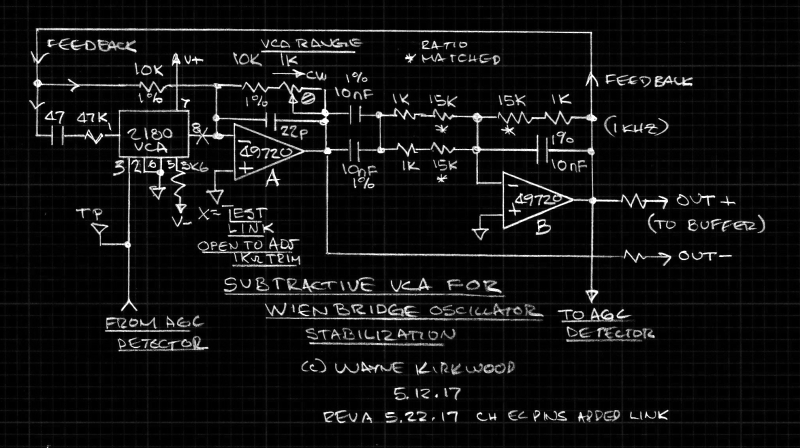
Subtractive VCA Stabilizes Wien Bridge Oscillator Rev A.
With the link open the pot is trimmed so the oscillator has just enough gain to start. (The 1K can be made much smaller in value maybe about 200Ω.)
With the link closed the final trim adjustment can be made by setting Ec- to +380 mV. This sets the VCA Q-point to about -63dB attenuation.
The AGC is a modified version of Vicktors Mickevics' half-wave design.
It was found that after the heavy filtering Vicktors' half-wave design had just as low a distortion as a full-wave rectifier. Its also very simple. Using the VCA the "kick-start" power-up circuit is not needed.
The whole oscillator - excluding output buffers - is just two LME49720 and a THAT2180 VCA.
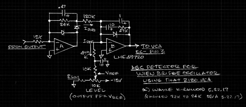
AGC Circuit for A Subtractive VCA_Stabilized Wien Bridge Oscillator.
Op amp A is a filtered half-wave rectifier which produces a positive output for negative-going inputs. It has a gain of 1.47. The output of the half-wave rectifier is converted to current by the 120KΩ resistor.
The AGC loop servo point is the inverting input of Op Amp B. Current is pulled out of the summing node by the output level adjustment. The oscillator output level is controlled by the servo action of op amp B and the VCA so that average current sourced from the rectifier hold the two opposing currents in equilibrium.
With the values shown, the oscillator output peak-to-peak level is equal to the reference voltage at the wiper of the output level pot.
At this point I'm measuring converter distortion.
I need to build the notch filter and add the TL431 shunt supply.
The updated Wien bridge oscillator schematic has a link added to disconnect the VCA output in order to preset the gain trim.
I'm also using the VCA Ec- pin and I increased the input resistor to 47KΩ.
Subtractive VCA Stabilizes Wien Bridge Oscillator Rev A.
With the link open the pot is trimmed so the oscillator has just enough gain to start. (The 1K can be made much smaller in value maybe about 200Ω.)
With the link closed the final trim adjustment can be made by setting Ec- to +380 mV. This sets the VCA Q-point to about -63dB attenuation.
The AGC is a modified version of Vicktors Mickevics' half-wave design.
It was found that after the heavy filtering Vicktors' half-wave design had just as low a distortion as a full-wave rectifier. Its also very simple. Using the VCA the "kick-start" power-up circuit is not needed.
The whole oscillator - excluding output buffers - is just two LME49720 and a THAT2180 VCA.
AGC Circuit for A Subtractive VCA_Stabilized Wien Bridge Oscillator.
Op amp A is a filtered half-wave rectifier which produces a positive output for negative-going inputs. It has a gain of 1.47. The output of the half-wave rectifier is converted to current by the 120KΩ resistor.
The AGC loop servo point is the inverting input of Op Amp B. Current is pulled out of the summing node by the output level adjustment. The oscillator output level is controlled by the servo action of op amp B and the VCA so that average current sourced from the rectifier hold the two opposing currents in equilibrium.
With the values shown, the oscillator output peak-to-peak level is equal to the reference voltage at the wiper of the output level pot.
At this point I'm measuring converter distortion.
I need to build the notch filter and add the TL431 shunt supply.
Last edited:
I now have an AGC loop that I'm happy with based on an adaption of Vicktors Mickevics' excellent design.
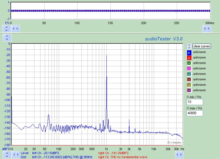
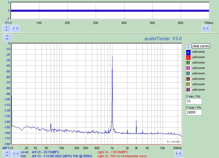
You have some hum sidebands on the 1k tone. The old SSM VCA worked for Jeff Smith and I, I figure the -130dB we got was just the op-amps and passives we had at the time. The best we got was using thermal feedback but was unusable due to settling time of minutes.
You have some hum sidebands on the 1k tone. The old SSM VCA worked for Jeff Smith and I, I figure the -130dB we got was just the op-amps and passives we had at the time. The best we got was using thermal feedback but was unusable due to settling time of minutes.
I was just looking at the AD536 RMS to DC converter again today (I use it in the autoranger) and wondered if it wouldn't be a good solution to derive the level control signal for these oscillators? At 1kHz the ripple on the DC output can almost be made arbitrarily small, especially with a 2-pole filter, and settling is fast.
Did anybody here ever consider this?
Jan
I was just looking at the AD536 RMS to DC converter again today
I'm in possession of the blessed reference AD536 that the trim engineer selected as close to perfect on all specs. This is a good idea actually.
I'm in possession of the blessed reference AD536 that the trim engineer selected as close to perfect on all specs. This is a good idea actually.
Just curious, is AD still running batches of this device in their foundries, or is there a good stock of devices/wafers and when it's done, it's gone?
The high price suggests the latter, these must be in an ancient process. Maxim did so with the MX536 (pin-to-pin equivalent), and after a few years it just vanished in thin air, leaving AD apparently the one and only source.
Just curious, is AD still running batches of this device in their foundries, or is there a good stock of devices/wafers and when it's done, it's gone?
I honestly don't know, there were some serious customers like Fluke that would justify a few lots now and then. This product was on 4" wafers originally, if transferred to 6" it could conceivably be run. There are products that were never entered into any digital system where the masks are still archived as rubylith. If a customer has an issue there are no sim files, no models, just hand drawn everything.
EDIT - Jan, if you need some I have a private stash N (very) OS. Waly I have Jarry's complete works in the original French, quite a guy.
Last edited:
There are products that were never entered into any digital system where the masks are still archived as rubylith.
Assuming rubilith is that red peeling stuff on a mylar sheet I've learned about, as being used in the 60's, how would you get it today to a 10:1 or 5:1 reticle? Is there any precision photo bench to transfer (with a reduction) the rubylith image to a photo plate still in operation today? I though those are already in the history manuals...
It was intended more like a hint about Mr. David Thomas.
Assuming rubilith is that red peeling stuff on a mylar sheet I've learned about, as being used in the 60's, how would you get it today to a 10:1 or 5:1 reticle? Is there any precision photo bench to transfer (with a reduction) the rubylith image to a photo plate still in operation today? I though those are already in the history manuals...
I suspect by now there was some scanning and digitizing involved. My memories are from a transition period already 20yr. ago where there were issues. We did draw the layers by hand and cut them into that red peeling stuff, the AD524 was done that way HP35 "sims", a real breadboard, then right to the drafting table. I listened to the Modern Dance last week, I was instantly converted in 1977 when REO Speedwagon and Kansas were the radio thing.
EDIT - Waly you jog my memories, I remember back in the ruby peeling days cranking "Life Stinks" to drown out the stupid muzak they piped into the lab.
Last edited:
You have some hum sidebands on the 1k tone.
Not anymore. (At least not big ones.)
Added some additional R bypass on the supply and used my super-duper foil/cardboard sandwich shield.
The Wima 10 nF 1% polys do pickup stray hum.
Still think I'm at the limit of the PCM4222.
VCA-Based Ultra Low Distortion Oscillator Mickevics Detector Shielded
131kpt FFT 10 sample average.
I also changed the half-wave rectifier's feedback resistor to 24KΩ to improve the Vref vs. P-P output scaling. (If that's important.)
Last edited:
cranking "Life Stinks" to drown out the stupid muzak they piped into the lab.
Yeah, I used "Final Solution" last week to get rid of some lab buggers post-beatniks, hunting my 40GHz VNA. After the first run, they took a half day off.
i worked at a company where in the next room they were cutting rubylith mask layers for 1K dynamic MOS RAM chips. I was told that a great skill was the ability to count accurately. I think they made it to 8K or 16K with rubylith. That would be quite the accomplishment given the process.
The chances of finding the hardware to photograph one of those rubylith masters would be really unlikely today. They were huge- 8'X 10' or more cut on an enormous light table with a glorified drafting machine to guide the process. That was the days of 2" and 3" wafers. At least the ovens and the rest of the machines were down one floor. Real vertical manufacturing- chips at one end of the building and monitors at the other end.
The chances of finding the hardware to photograph one of those rubylith masters would be really unlikely today. They were huge- 8'X 10' or more cut on an enormous light table with a glorified drafting machine to guide the process. That was the days of 2" and 3" wafers. At least the ovens and the rest of the machines were down one floor. Real vertical manufacturing- chips at one end of the building and monitors at the other end.
Still think I'm at the limit of the PCM4222.
I'm pretty sure you are. That's around the best I got from that board. Either a passive notch (there are several variants floating around here) or an AKM based ADC. Victor's oscillator usually has -150 dB harmonics which is well below any ADC I know of. With a good implementation the AK5394A you can get to approx -130 dB harmonics.
- Home
- Design & Build
- Equipment & Tools
- Low-distortion Audio-range Oscillator