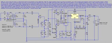
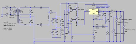
I went ahead and cascaded the two mosfets.
In the schematic they're 800 V units, but the real ones I'll use are 1KV each, with about the same gate charge.
The circuit runs fine in LTspice. I'm just asking if you guys would take a look at the schematic and give me feedback on whether the two mosfets are cascaded "properly"...I just used the same signal to drive both gates...the ramp up is decently soft.
I need both NMOS to split the dissipation equally; since they're inside the same loop, in series...I think...I think that happens automatically, but I'd like a double-check.
The main reason for putting in two is just voltage headroom; I don't want voltage spikes from the SS/RC stage blowing the mosfet.
Best, Charlie
Attachments
@Gary P, (or someone else more skilled than myself🙂)
Looking for parts to build the Swenson Regulator I found a large quantity of the SEC IRFS820A mosfet. It's sort of similar to the IRFS820B but gate-to-source voltage is circa 30V. Can this part be implemented in the design, and -in case it can- which parts need to be altered?
Looking for parts to build the Swenson Regulator I found a large quantity of the SEC IRFS820A mosfet. It's sort of similar to the IRFS820B but gate-to-source voltage is circa 30V. Can this part be implemented in the design, and -in case it can- which parts need to be altered?
Lots of great information guys!
Thanks for the posts Gary!
If there is going to be a group buy of some description, I would be interested...
Now for a few more dumb questions (no such thing as a dumb question - just dumb people...), Mentioned above was the use of either a CRC or CLC filter on front end of the reg. What is the advantage of using a choke instead of a resistor? If ripple is not that great of a concern, a CRC with 30uF, 150R, 220uF gives less than 2V ripple and the resistor dissipates around 5 watts of heat. Choke gives better ripple reduction, but costs around $35 in stead of a buck or two and uses up a ton more chassis space. Is using a choke then overkill if we are regulating anyway?
Next question, Gary mentioned getting 400volts regulated from 625v in. I am after 400 volts regulated too, but have 400-0-400 to start with. I figure that as they are Hammond 300BX transformers, I am going to get some overvoltage, and am figuring on about 500volts rectified. I am hoping that is OK, 490v mentioned previously as a minimum...
For Charlie, Thanks for the guidance, I appreciate it. This amp is not my first, just my first regulated tube amp. Have built a chip amp with a regulated supply and have built about half a dozen tube amps with unregulated supplies. This amp is going to be a 7591 PP with Tamura output iron, hence looking at quality power supply and driver circuitry.
Disco,
AFAIK you can change IRFS820B without any significant changes to the circuit - from reading the Swenson regulator notes on GP's site - changing to a 900V FQAF11N90 mosfet required a change to the gate R (from 100 to 47 ohm) & ensure the at least 10mA draw at chosen voltage.
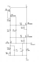
Here's an explanation of the original Swenson regulator's workings from John Swenson: I've attached his original regulator before Gary Pimm added the current limiting parts & other tweaks.
AFAIK you can change IRFS820B without any significant changes to the circuit - from reading the Swenson regulator notes on GP's site - changing to a 900V FQAF11N90 mosfet required a change to the gate R (from 100 to 47 ohm) & ensure the at least 10mA draw at chosen voltage.
Here's an explanation of the original Swenson regulator's workings from John Swenson: I've attached his original regulator before Gary Pimm added the current limiting parts & other tweaks.
On the right side is a cascoded source follower. The voltage on the bottom (source) of Q1 follows the voltage on its gate minus about 4 volts or so. (if the gate is at 100V the source will be at 96V). The exact difference between the gate and the source will vary somewhat depending on the current flowing through it and the voltage across the transistor. The second is handled by Q2. It’s called a cascode, it maintains a constant voltage across Q1, any difference in the input voltage is developed across Q2, thus preventing it from changing the gate to source voltage of Q1.
The left side is in charge of producing the voltage references to drive the gates of Q1 and Q2. This is done by Q3 and Q4 which form their own high quality low current (0.33mA) CCS. This current flows through R14, R10 and R11 developing constant voltages across them. (R17 is part of the CCS) The voltages can be changed by changing the resistor values.
R10 and R11 comprise the main voltage reference. They are filtered by C2 to make a low noise reference. R14 is the cascode bias. It determines the voltage difference between Q1 and Q2. As described so far this is the original Gary design. The Q3/Q4 CCS performs two functions, main voltage reference and cascode bias.
The modification to a feedback regulator is done by adding Q5. This is basically a comparator, one input is the reference voltage underneath it, the other is the output voltage. The "output" is the drain of the MOSFET which drives the gate of Q1. The beauty here is that the same CCS that provides the constant current for the references is also the CCS load for the error amplifier! The same CCS is being used for three different tasks. Most error amplifiers just use a resistor load for the amp, but they work even better with a CCS load, but that is rarely done because of the extra complexity of the CCS load. Because one was already in Gary's design it was a piece of cake to have a CCS loaded error amp.
This error amp takes care of the changes in gate to source voltage caused by current fluctuations from the load. The result is very good regulation no matter what the load is doing.
Attachments
Hello jkeny, thanks for helping out here.
John Swenson's text indeed gives insight in operations. One thing unexplained remains why R15 needs to be decreased when changing IRFS820B to FOAF11N90C. Is it because of higher Vgs or because of higher cascoded source follower current?
Locating LND150 without a credit card seems troublesome. Do you perhaps have a quantity to sell? I can swap them for 820A's 🙂
Right now I'm finishing a single sided 'low voltage' board (without the high voltage zenerdiodes) but wondered about the cascode capacitor (C5). From the pictures it seem Gary uses a electrolitic capacitor. Would a polarised cap of 1uF/250V be suitable?
Best regards
Chris,
To my opinion it's not necessairy to deliver smooth DC to the reg, ripple of 1 or 2 volts will be acceptable. As long as the output voltage of your powersupply is high enough to withstand mains fluctuations plus voltage drop in the regulator you're safe. The question is how much voltage does the regulator need for stable operation? Maybe we find Gary willing to tell us something about it... or build it and find out by testing 😉
To my opinion it's not necessairy to deliver smooth DC to the reg, ripple of 1 or 2 volts will be acceptable. As long as the output voltage of your powersupply is high enough to withstand mains fluctuations plus voltage drop in the regulator you're safe. The question is how much voltage does the regulator need for stable operation? Maybe we find Gary willing to tell us something about it... or build it and find out by testing 😉
Jaap,
I don't have any to spare, sorry - I ordered mine through a fellow DIYA member in the US to minimise shipping & any taxes.
I think R15 is just a gate stopper R that is necessary on mosfets to prevent oscillation - don't know why the change.
C5 is a low voltage (50V) electrolytic cap (with the + towards Q5) in the original Swenson schematic I posted above.
GP did some tests and as a result tweaked it a bit to the schematic attached. He added some current limiting (Q6,R4,R3,R1), short circuit protection (CR1, VR3) & high voltage operation (Q7, VR5,VR6,VR7) & some performance tweaks (R14 to 56K, C2 to 4.7uf)
Attachments
Hi Chrish,
What you really want to do is deliver what looks like a low frequency sine wave type ripple to your regulator circuit. That, it can get rid of easily.
How you decide to do this is up to you. 😉
-Chris
No. The choke is much better at reducing the higher frequency components of noise. That's something that all solid state regulators do less well than what they can do at 100 or 120 Hz.Is using a choke then overkill if we are regulating anyway?
What you really want to do is deliver what looks like a low frequency sine wave type ripple to your regulator circuit. That, it can get rid of easily.
How you decide to do this is up to you. 😉
-Chris
Some answers...
R15, the resistor on Q2 is more than a just a gate stopper. It is actually tuning the speed of the MOSFET cascode circuit. If the value of R15 is too high, the circuit will oscillate in the 150Khz to 250Khz range with what looks like a relaxation oscillator. If the value of R15 is too low the circuit breaks into a chaotic high frequency oscillation that my Tektronix TDS460 scope can't trigger on well enough to get a frequency measurement.
This behavior has been constant with the CCSs, the amplifier modules, and the regulator circuit. The value is chosen to be at the approximate mid point between the 2 modes of oscillation.
In the self bias and battery bias CCS circuits when using the IRF820a parts the Q2 gate stopper was 2.2K. When the IRF820B came out the value had to be increased to 4.7K as the IRF820B is a faster part. Using the FQAF11N90C in the regulator required lowering the value of R15 to 47 ohms as the FQAF11N90C seems to be slower than the IRFS820B. The regulators use lower value resistors because of the insertion of the error amplifier, Q5. Using an IRF820A may require lowering the value of R15 to match the speed of the part. I don't have any more of the IRF820A parts to play with. I shy away from the SEC parts as the only bad batch of MOSFETs I got was from SEC.
C5 in the latest version of the regulator has dropped down to a .1uf film cap and gets connected to the Q1 side of R1. The board layout does not support the new connection point for C5 so you need to connect it up as shown in the photo at the end of the regulator page.
As for minimum voltage, when the total voltage drop across the regulator is down to 50 volts the performance is starting to drop as the various capacitance's of Q2 are increasing. IIRC the ripple rejection at 50 volts was down to merely 105dB from the 120dB with 100 volts drop. Regulation pretty much stops at 25 volts or less drop.
Charlie, I'm not sure what you are trying to do with the dual MOSFETs. If you want them in series you will need a voltage divider on the gate of the upper MOSFET to bias it to half the voltage you want to drop across both MOSFETs. As drawn with both gates referenced to the same voltage the upper MOSFET will get all the voltage and the lower MOSFET will not have any voltage to turn on. The biggest error in your schematic is not having any protection zener diodes on the gates of the MOSFETs. In a circuit like this no protection zeners is a guarantee for dead parts. Most MOSFETs can only tolerate +/- 20 volts on the gate. Some of the newer MOSFETs can handle more but you have to check the data sheets to know.
I agree with Chris about the choke. Even though the regulator performs very very well, the cleaner the input is the less junk there is to regulate out.
Thanks Gary for your post - explains a lot - just one question, how can R15 be calculated or assessed in circuit - does this require a scope or are there any other methods of determining high/low values for R15?
I determine the value for R15 by placing a pot in the circuit then noting where the oscillations occur using a scope. When doing this you run the load current up and down and vary the voltage drop across the regulator to make sure the chosen value works over the full range that is wanted.
I'm have used STP4NK60ZFP mosfets in my 2 Swenson regs that I've constructed. These are 600V 4A 25W Total ON speed 21ns Off 45ns. I've used 100 ohm for R15 as the speed seems close to IRFS820B ON speed 40ns OFF 75ns.
I'm using the regs in a Swenson BDT preamp which I'm building so the vreg outputs are 240V & 130V. My PS is 310V DC.
I don't have a scope - is there another way to determine whether the circuit is oscillating or not - parts heating, etc?
I'm using the regs in a Swenson BDT preamp which I'm building so the vreg outputs are 240V & 130V. My PS is 310V DC.
I don't have a scope - is there another way to determine whether the circuit is oscillating or not - parts heating, etc?
jkeny, can't help you with that.
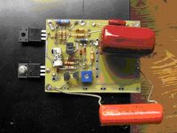
Waitin' for semi's to arrive...
Waitin' for semi's to arrive...
An externally hosted image should be here but it was not working when we last tested it.
An externally hosted image should be here but it was not working when we last tested it.
An externally hosted image should be here but it was not working when we last tested it.
Nice boards Jaap,
What software did you use to design? Did you etch them yourself?
Edit: it's probably perfectly fine but R15 & R7 need to be as close to the gates as possible to also stop any oscillations.
What software did you use to design? Did you etch them yourself?
Edit: it's probably perfectly fine but R15 & R7 need to be as close to the gates as possible to also stop any oscillations.
Thank you. I use Eagle to place components but have a hard time getting proper routing with it. Maybe I should practice more. What I do next is making a 1200dpi master with Photoshop based on the Eagle output. Labor intensive but that way you get it exactly you want it.jkeny said:Nice boards Jaap,
What software did you use to design? Did you etch them yourself?
The pump of my etch tank died since last use so I used a heavier one. Seems it does it's job a little to good 🙂
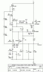
C0 is integrated to bypass the power supply as it's 20cm away. Also I've split the voltage reference because the unit will not be adjustable in future. I'm not quite shure about the power in R3, do you know on what voltage it will be?
I like the way you include the pinouts of the parts on the schematic - is this just cut & paste from datasheets?
I saw C0 - good idea. R3 is just a 0.5W rating afaik. You can tell a lot from Gary's Pic
I think there is a problem at the C5 R15 junction - this should be connected to the gate of Q3 and then to the junction of R17 & R14
I saw C0 - good idea. R3 is just a 0.5W rating afaik. You can tell a lot from Gary's Pic
I think there is a problem at the C5 R15 junction - this should be connected to the gate of Q3 and then to the junction of R17 & R14
Attachments
Thanks for pointing out the fault. A piece of wire will do, fortunately.jkeny said:I like the way you include the pinouts of the parts on the schematic - is this just cut & paste from datasheets?
I saw C0 - good idea. R3 is just a 0.5W rating afaik. You can tell a lot from Gary's Pic
I think there is a problem at the C5 R15 junction - this should be connected to the gate of Q3 and then to the junction of R17 & R14
Yes, it's cutting and paisting from the datasheets. Apple computers have a nifty tool for that. With Microsoft there's more to it but still possible.
Gary,
Thanks for the info.
Yeah, when I found out how to measure power in each component in LTspice I realized that biasing scheme was wrong. Ooops.
I made a new biasing scheme for both mosfets, and now they share power fairly well.😀
It works well now; output impedance is in the vicinity of 20 milliohms, not that it matters much. It maintains regulation up to about an amp, at which point the limitations of the power transformer kick in...I'll have to run a sim with a current-limitless sine wave voltage source just for kicks, it should maintain regulation until the silicone dies melt
The circuit as shown has a very heavy, complex load, much heavier than it will actually see in the amp. And, I'm making one for each channel, so the actual load on each one will be even less.
I got rid of the cap at the LM317 input, there's just no good way to save the LM317 in a short with a cap on it's input without introducing additional output impedance.
Nonetheless, I still need to add current limiting for short-circuit protection. I don't want to add a current limit resistor between the second mosfet and the LM317, as Maida did, so it will have to be a circuit which pulls down the gates of both mosfets very quickly, I think. Since they're already acting as roughly tracking pre-regulators, I think that strategy should work well.
In real life, I may have to reduce the gate stoppers, but we'll see. Enhanced NMOS, I think, does better with large gate stoppers than Depletion NMOS.
Best, Charlie
P.S.: I just remembered the circuit as shown has a 100uF cap on the reg output, but the simulation was done with a 0.1uF cap there; I just like as much capacitance on the output as possible. Doesn't make any difference in the output impedance, so it may be money wasted, dunno, but the consensus seems to be that amps sound better with more capacitance on B+...but...I think this may only be true with higher impedance supplies.
Attachments
Which also reminds me....
Your point about the protection zeners for the mosfet gates is well taken, but it makes me feel a little like Broskie when someone writes in telling him he left a protection diode out...but you're right, someone not familiar with mosfets wouldn't know to add the gate protection.
The mosfets I am actually going to use have internal zeners for gate protection. When I use non-protected mosfets, I always put two opposed 18 volt zeners in series from gate to source.
The mosfets shown, the closest model I have, don't have internal zeners, so technically I should have put the gate protection zeners in, but I didn't want to clutter up the schematic more than it already was.
For example, I finally decided to go with a can cap with base clamp for the input cap instead of the shown series'd cap rig with voltage balancing resistors, but never got around to simplifying the schematic there.
If a beginner wishes to make this regulator, I'd advise two things: let me know, so I can give you a fully-protected circuit based upon your specs and device-choices, and wait until I've actually bench tested it instead of just a simulation.😎
Best, Charlie
There's a lot reading involved concerning oscillation, but you might try a google on Barkhausen criteria.jkeny said:... I don't have a scope - is there another way to determine whether the circuit is oscillating or not - parts heating, etc?
- Status
- Not open for further replies.
- Home
- Amplifiers
- Tubes / Valves
- Look for high-voltage regulator projects