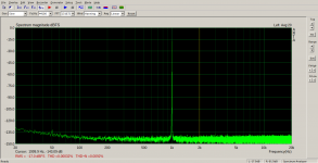
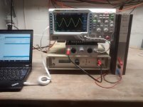
To estimate the actual measuring headroom I did a loopback measurement with the EMU-tracker in use.
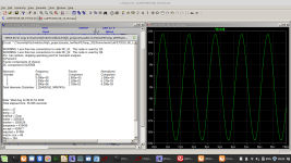
H1/H2 = -17 -(-143) = -135 dB. H2 disappears in the noise floor. So there is still some measuring headroom for further improvements.
H1/H2 = -17 -(-143) = -135 dB. H2 disappears in the noise floor. So there is still some measuring headroom for further improvements.
Attachments
Last edited:
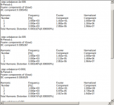
In the meantime I had an idea to simulate H2 distortion induced by output current imbalance. A small resistor is inserted into the output current summing node that generates a tiny voltage offset under current flow. The measured output is connected to one terminal of this resistor while the feedback input is connected to the opposite terminal.
Attachments
And this is the result of the simulation stepping imbalance resistor through 0.000001/0.00001/0.0001 Ohms
This confirms that H2 distortion is extreme sensitive against tiny imbalance of the copper trace layout.
And for the even harmonics lovers here - inserting this resistor enables you to add even harmonics at your gusto!
This confirms that H2 distortion is extreme sensitive against tiny imbalance of the copper trace layout.
And for the even harmonics lovers here - inserting this resistor enables you to add even harmonics at your gusto!
Attachments
Last edited:
Hehe, good point! At the time there is one single PE connection, anyway it may be wise to connect this elsewhere.Watch for shorted turn on mains transformer with that connection to the mounting bolt
Last edited:

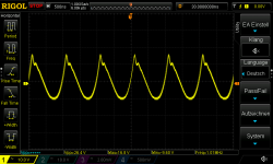
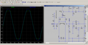
500kHz is heavily distorted looking more than a triangle. So I simulated the actual circuitry and LTSpice showed similar results. Fiddling a bit in LTSpice I discovered that the compensating network is of great influence here.
Attachments

Last edited:
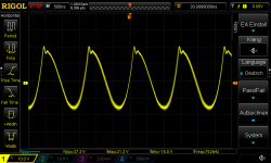
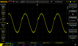
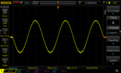
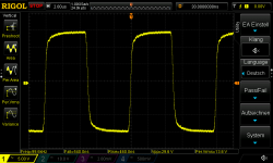
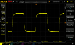
Consequently I modded the real circuit accordingly. With improved results. The following scope screenshots are taken at constant input level and 10R load.
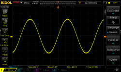
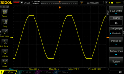
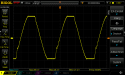
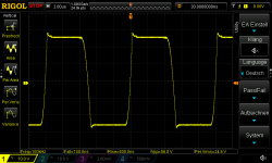
Frequencies are 100k, 250k, 500k, 600k, 750k, 1MHz.
Doubling VAS bias current did not show any improvement in LTSpice so this remains at approx 13mA.
Frequencies are 100k, 250k, 500k, 600k, 750k, 1MHz.
Doubling VAS bias current did not show any improvement in LTSpice so this remains at approx 13mA.
Attachments
-
 LatFETamp_2019_08_14_1000kHz_26Vpp_10R_load.png32.6 KB · Views: 58
 -
 LatFETamp_2019_08_14_0750kHz_37Vpp_10R_load.png35.2 KB · Views: 52
 -
 LatFETamp_2019_08_14_0600kHz_39Vpp_10R_load.png31.1 KB · Views: 299
 -
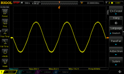 LatFETamp_2019_08_14_0500kHz_40Vpp_10R_load.png30.1 KB · Views: 306
 -
 LatFETamp_2019_08_14_0250kHz_43Vpp_10R_load.png30.3 KB · Views: 297
 -
 LatFETamp_2019_08_14_0100kHz_46Vpp_10R_load.png29.9 KB · Views: 308
Hehe, good point! At the time there is one single PE connection, anyway it may be wise to connect this elsewhere.
Yes, definitely! I can see why its convenient to reuse that bolt for PE, but it's
asking for disaster (not to say mains hum!)
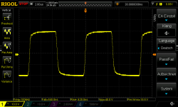
PE is re-routed to the heatsink. The VAS needed slight adjustment for symmetrical current drive (R6=150R||1k5). The following screenshots show clipping behaviour with 10kHz and 100kHz sinewave, respectively.
Attachments
Measuring square response at 100kHz with 20, 30, 40, 56Vpp output signal feeding 10R dummy load. The last measurement is overdriven.
Attachments
The recovery from the negative rail has a hiccup, I suspect that's due to the VAS transistor saturating. Current limit transistor across R6 on that might help (and protect the VAS transistor from cooking and make the current drive symmetric without having to compromise the VAS transconductance much)
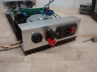
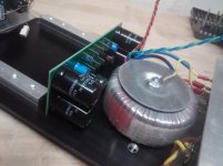
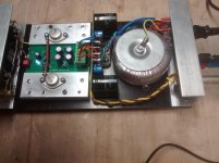
The power supply is basic. A 2x24V/80VA toroidal xformer, bridge rectifier and 2x2x2200uF/63V bulk caps feed the main circuit. Two charge pumps add 8,5V to both aux supplies. Thus the gate voltages swing includes the rails plus clamping diode forward drop - minus BE drop of the emitter follower buffer - at the end supply rails.
Last edited:
Yes, that looks a bit ugly. But the simulation shows limited VAS current as is. And the clamping diodes should prevent the VAS from saturation. I would be happy if the neg recovery would look as nice as the pos one, but actually I do have no idea how to achieve that. If you want to investigate I append the latest asc here.The recovery from the negative rail has a hiccup, I suspect that's due to the VAS transistor saturating. Current limit transistor across R6 on that might help (and protect the VAS transistor from cooking and make the current drive symmetric without having to compromise the VAS transconductance much)
Attachments
Last edited:
Playing with the sim I came to the conclusion that clipping recovery here is not caused by regular recovery from bjt saturation (turn-off-delay) but is a matter of general recovery from clipping overdrive back to normal operation in the voltage controlled current source of the VAS. In that case it is more like a turn-on-delay.
Last edited:
- Home
- Amplifiers
- Solid State
- Just another lateral FET amp