Increasing the emitter degeneration resistors of the LTP from 0 to 100R speeds up recovery from clipping - at the expense of reduced loop gain.
There is no free lunch...
There is no free lunch...
Attachments
Last edited:
Shutting down the soldering iron and back to LTSpice. Luckily this overshoot appeared in the simulation as well. After fiddling at different locations it turned out that an additional capacitor of 3n3 between both emitters of the input differential pair was the solution. Presumably this gives some additional phase boost to the loop thus reducing loop overshoot.
But the verification of this promising patch was delayed by some heavy trouble shooting: While increasing the gain of the scope I discovered substantial noise that finally could be triggered - the frequency was close to 200MHz! The strange thing was that I could not discover high voltage excursions anywhere in the amp. But with a simple H-field sniffer there were circulating currents found in the vicinity of the pcb. Finally the source was located in the area of the gate drive circuitry and the beast could be tamed parallelling a 47~100pF to the CE-terminals of the PNP gate driver.
But the verification of this promising patch was delayed by some heavy trouble shooting: While increasing the gain of the scope I discovered substantial noise that finally could be triggered - the frequency was close to 200MHz! The strange thing was that I could not discover high voltage excursions anywhere in the amp. But with a simple H-field sniffer there were circulating currents found in the vicinity of the pcb. Finally the source was located in the area of the gate drive circuitry and the beast could be tamed parallelling a 47~100pF to the CE-terminals of the PNP gate driver.
Attachments
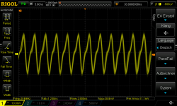
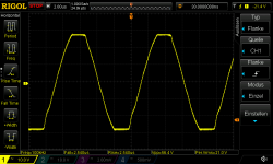
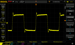
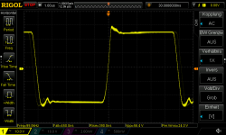
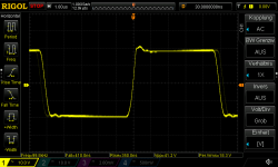
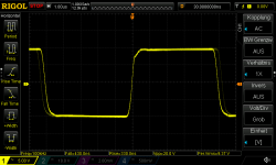
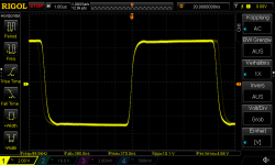
After this annoying episode the modifications could be verified successfully. The screenshots depict 100kHz square response into 10R dummy load at 10, 20, 30, 40 and 50Vpp output level.
Attachments
-
 LatFETamp_2019_08_15_100kHz_50Vpp_10R_load_Re_100R_39p_3n3_100p_10R.png29.8 KB · Views: 115
 -
 LatFETamp_2019_08_15_100kHz_40Vpp_10R_load_Re_100R_39p_3n3_100p_10R.png27.9 KB · Views: 115
 -
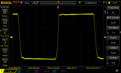 LatFETamp_2019_08_15_100kHz_30Vpp_10R_load_Re_100R_39p_3n3_100p_10R.png29.4 KB · Views: 105
 -
 LatFETamp_2019_08_15_100kHz_20Vpp_10R_load_Re_100R_39p_3n3_100p_10R.png27.7 KB · Views: 116
 -
 LatFETamp_2019_08_15_100kHz_10Vpp_10R_load_Re_100R_39p_3n3_100p_10R.png29.5 KB · Views: 363
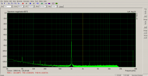
And back again to ARTA and STEPS. This distortion spectrum was measured at 17Vrms output into 10R dummy, just 1dB below the onset of clipping. THD is at the limit of my test equipment. And despite the simple unregulated power supply there is very little hum which indicates a superior supply rejection.
Attachments
Last edited:
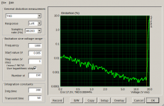
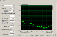
The next plots show THD versus output voltage at 1k/6kHz respectively. The abrupt transition from THD sweetspot into hard clipping is typical for an amplifier with a very high loop gain.
Attachments
Last edited:
Last edited:
Very nice achievement and very good results!
Which I had your skills regarding trouble shooting.
Which I had your skills regarding trouble shooting.
Thank you for the kind words. And yes, after a lifetime of experience troubleshooting is still the biggest headache 😀Very nice achievement and very good results!
Which I had your skills regarding trouble shooting.
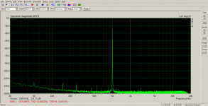
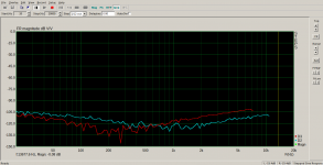
Noise performance measurements were a bit too optimistic because in the meantime I had swapped differential pair emitter degeneration resistors from 0R to 100R. This degrades noise performance slightly. But at first I had to struggle with 50Hz hum around -75dBV with input shorted (potentiometer set to min). Replacing the 2u2 Wima input coupling cap by a 100u/16V elelectrolytic solved this problem. The plot shows output noise measured at left channel. The right channel unused serves for comparision with the soundcards intrinsic noise floor.
Attachments
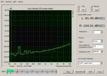
-91.45dBV vs -93.2dBV computes to 1.75dB reduced S/N - this matches perfectly my expectations. Output noise voltage is 27uVrms now and dynamic range is 116dB - not too bad at all!
Last edited:
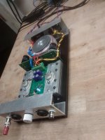
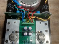
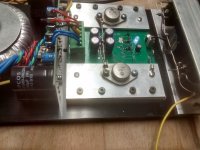
So I did some fine-tuning of the wiring. The power-MOSFET sources summing node was relocated to the other pair of TO-3 fixing screws thus increasing the distance to the input stage. This further improved harmonic distortion as can be seen by the latest plot of 1kHz, 15Vrms into 10 Ohms.
Attachments
Last edited:
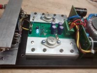
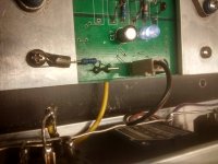
The photographs depict actual wiring of source summing node, PE to AGND connection and general wiring
Attachments

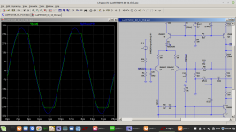
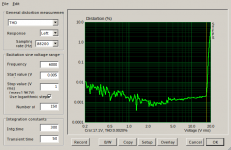
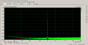
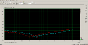
To evaluate THD vs frequency I used ARTA/STEPS. It turned out that measurements beyond 20kHz do not work with my soundcard, even at a sampling rates of 192kHz. The anti-aliasing filters are not switched accordingly so I measured with the sample rate of 44.1kHz upto 20kHz. The graph on top is the signal level, normalized to about 0 dB. The harmonics "D2" and "D3" appear in the region of -100~120dB and increase slowly with higher frequencies.
Attachments
- Home
- Amplifiers
- Solid State
- Just another lateral FET amp