Yes, but I don't know whether the higher transconductance of the puck is advantageous in this situation. It seems to me that since we want to limit the contribution of the mosfet, the lower transconductance may be welcomed. In any case I do not need the dissipation capacity of the puck.
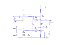
Just to finish it off, the signal peak to peak current through R10 was 450mA, from mosfet toward SIT. Current at SIT drain was 274mA. Adding the two is 724mA, which is close to the 719mA through C4.
So the currents seem to sum up properly. From what I can see, output signal from the mosfet exits through C7 and C4.
That's my amateur DIYer's perception - may or may not be the truth. 🤓
So the currents seem to sum up properly. From what I can see, output signal from the mosfet exits through C7 and C4.
That's my amateur DIYer's perception - may or may not be the truth. 🤓

The resistors and capacitors mentioned in posts #419 and #422 are shown in the schematic in post #414.
From post #44.The power supply is single ended, but that is not of interest here. Any conventional voltage gain stage for a front end will "work".
The interesting thing is the complementary circuit which biases the output SIT.
Maybe I will post that on Christmas...

Apparently the grinch stole the "complementary circuit which biases the output SIT".

Just catching up with pieces of this thread. Did Stan Ricker the mastering engineer also do design work for JBL?
As I know it, Greg Timbers is the man from about '73 to a few years ago.
And a nicer guy does not exist...
And a nicer guy does not exist...
Last edited:
That name is more familiar there. I was just going by your post 167 on the cap bias. I remember Jung and Marsh covering that trick to some degree.
I have been thinking of a simple way to bias the mosfet.
If you have hundreds of SITs to choose from, maybe you can find SITs that have a high Vgs, higher than the Vgs of the mosfet plus the voltage difference between the SIT and mosfet sources.
I don't have hundreds of SITs though. 🤓

If you have hundreds of SITs to choose from, maybe you can find SITs that have a high Vgs, higher than the Vgs of the mosfet plus the voltage difference between the SIT and mosfet sources.
I don't have hundreds of SITs though. 🤓
considering that there is common source resistance (ensuring increased thermal stability), I'm sure that Redneck biasing scheme is more than adequate
and, that's just one of ways .......
and, that's just one of ways .......
A simple solution to both bias and to adjust the mosfet as a current source to increase or decrease its contribution easily would be brilliant. 😎
Here is something to think about:
The image shows a sequence of equivalent circuit transformations of the SIT5 Output Stage. The sequence is ordered left-to-right, top-to-bottom. Simulations verify the correctness of these equivalent circuits.
The image shows a sequence of equivalent circuit transformations of the SIT5 Output Stage. The sequence is ordered left-to-right, top-to-bottom. Simulations verify the correctness of these equivalent circuits.
Attachments
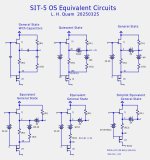
There should have been one more final transformation replacing the battery -z0 with the output capacitor.
For biasing purposes, the original schematic makes sense, but as a result of this analysis, I do not understand the importance of Papa's "ratio R1 and R2" statement".
For biasing purposes, the original schematic makes sense, but as a result of this analysis, I do not understand the importance of Papa's "ratio R1 and R2" statement".
- Home
- Amplifiers
- Pass Labs
- First Watt SIT5