Hi, Mike,
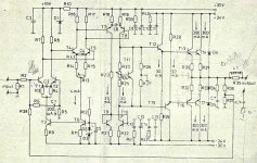
This is the schematic of one of the "best" sounding amp. It is Electrocompaniet 25W.
It has the topology like you use in Symasim, also do not use complementary differential, but has 1 additional differential from what you use.
What do you think this design wants to achieve by adding 1 more differential? Is it trying to get more OL gain? But trying to get more OL gain will result in lower OL bandwith?
Attachments
Mr Evil said:This is a good reason to use an improved, high gain Vas such as the EF buffered one that Self proposes, or a Sziklai pair, or a cascoded MOSFET. Doing so will yield an extremely high current gain to well past the audio band, minimizing distortion in the LTP.
I've noticed that people arguing against current mirrors neglect the base currents in the current mirror itself. If the base current of the buffer of the VAS can be arranged to be twice the base current of a single input stage mirror transistor (assuming a simple two-transistor mirror), the error will be zero.
Eva said:I've done the actual test and phase shifters doesn't behave as a true delay even in its valid frequency range.
Assuming a string of phase shifters, properly aligned in order to get a consistent group delay up to a certain frequency 'f', when you start feeding a sine wave of a frequency well below 'f' to such a string of phase shifters, the output reacts inmediately showing that sine wave with a very low amplitude that increases progressively until it matches the input amplitude.
The time it takes for the amplitude to sweep is what we could call 'simulated delay'. Note that this has absolutely nothing to do with delaying in time a waveform, though.
Hi Eva,
Could you please reveal the type of framework implemented by you in determining the response of phase shifters in their valid frequency domains.....
Hi PMA,PMA said:
And one must not forget to measure distortion spectra at low output levels and to take into account high order distortion components. That's where Self's amp fails. Error correction is necessary, optimal bias for AB as per Self is not enough.
Great said,..Every stage must be furnished to minimize the error generation and sometimes high bias eventually fails to eradicate the distortion artifacts in various amps, besides this there are many excellent amps exist with low biased output stages..
andy_c said:
I've noticed that people arguing against current mirrors neglect the base currents in the current mirror itself. If the base current of the buffer of the VAS can be arranged to be twice the base current of a single input stage mirror transistor (assuming a simple two-transistor mirror), the error will be zero.
Lets take an example in the case of cascaded differentials.
first differential collectors loaded by CCS[no current mirrors] and then followed by EF, then again followed by second differential acting as VAS with seperate CCS..
So what's your opinion in this case...
regards,
K a n w a r
That's something worth thinking about, but it doesn't account for the variation in Vas input current with frequency, which will increase much more than the mirror base current, nor the reflection of output stage nonlinearities back to the LTP via the Vas, which would also change the current so it no longer matches the mirror base current. I think it would be better to spend one or two extra transistors in the current mirror to cancel base currents.andy_c said:
I've noticed that people arguing against current mirrors neglect the base currents in the current mirror itself. If the base current of the buffer of the VAS can be arranged to be twice the base current of a single input stage mirror transistor (assuming a simple two-transistor mirror), the error will be zero.
D.Self is VERY wrong about the "poor" balancing in this topology
D. Self is wrong about some considerations. For example he claims that a CFI is more linear than an emitter follower as well when he stated that a dual output stage does not load the VAS. Read that article very carefully.
A dual diff pair is very sensitive for different currents in each currents in the LTP. As Mike has stated this loads only the VAS in a different way. Different currents can easily obtained by self heating of the dual diff. As in the dual diff the currents in left and right tail must be equal (by symmetry reasons), a thermal runaway is not uncommon. A reasonable solution is using generation resistors in the LTP as well as glueing the LTP transistors together
This is a good reason to use an improved, high gain Vas such as the EF buffered one that Self proposes, or a Sziklai pair, or a cascoded MOSFET. Doing so will yield an extremely high current gain to well past the audio band, minimizing distortion in the LTP.
To my experience not the VAS or LTP creates most distortion but the output stage. The main distortion mechanism is crossover distortion when the output stage is driven by a high impedance VAS stage. Most and to me useless discussion about linearity is made when the output stage is driven by a voltage source. This does not match the reality although a lot of simulation and theoretical examination has been done here (D. Self and also Prof. Leach. It is a good starting point but unfortunately not more. The models and presumptions they are using are too simple). The input impedance of a class AB output stage (when using BJTs) is very unlinear (look to D. Selfs article, this part is very good!) and modulates the open loop gain of the amp.
To my experience not the VAS or LTP creates most distortion but the output stage. The main distortion mechanism is crossover distortion when the output stage is driven by a high impedance VAS stage. Most and to me useless discussion about linearity is made when the output stage is driven by a voltage source. This does not match the reality although a lot of simulation and theoretical examination has been done here (D. Self and also Prof. Leach. It is a good starting point but unfortunately not more. The models and presumptions they are using are too simple). The input impedance of a class AB output stage (when using BJTs) is very unlinear (look to D. Selfs article, this part is very good!) and modulates the open loop gain of the amp.
That's a good reason to use low output impedance VAS isn't it?😀
bocka said:
The input impedance of a class AB output stage (when using BJTs) is very unlinear (look to D. Selfs article, this part is very good!) and modulates the open loop gain of the amp.
darkfenriz said:
That's a good reason to use low output impedance VAS isn't it?😀
Yes !
It took me long to understand why low zout of vas has such big
improvement to soundquality... The formulas showed by bocka
finally explained to me how these resistors to gnd in vas improved
the quality of my amps. This effect does not show up with sinewaves
or pure resistive loads, but with complex signals into reactive loads
you get a hell of IMD ! (Gives a very bright and glare / exaggerated
sound, sounding not bad, but wrong -> false trebles)
The more i think about it, the worse it gets... In theory it's even
possible to create resonances between amp and speaker ?
Mike
MIKEB
"The formulas showed by bocka finally explained to me how these resistors to gnd in vas improved the quality of my amps."
The fall in impedance using this technique is not very effective unless the resitances are very low, but then the distorsion of the VAS enhances due to more flowing current. The quality you think you get is in fact nothing other than more distorsion.
"In theory it's even possible to create resonances between amp and speaker ?"
Resonance would mean instability.
BOCKA
" The input impedance of a class AB output stage (when using BJTs) is very unlinear (look to D. Selfs article, this part is very good!) and modulates the open loop gain of the amp."
This modulation of the open loop gain is evident, but from various subjective reports, it does not seem to make so much harm. However, at least from the theorical point of view, I am all in favour of a minimal modulation of the open loop. So a logical technique is to enhance the current gain of the outpout stage. Using three transistors in each branch, there are numerous solutions :
- triple emitter follower
- feedback triple (Quand 303)
- a push-pull class A buffer using one NPN and one PNP, driving a conventional ouptut stage made of four transistors, either in emitter followers or in compound pairs. I wonder if this solution is not at least equivalent, or even much better, than to try to have a symetrical VAS stage.
- I recently got another idea which I have rarely seen done : a push-pull class A buffer using compound pair in each branch driving simple power NPN and PNP emitter followers. As there is a lot of current to charge and discharge the power transistors, the output should be fast and crossover distorsion low.
Note that B.J Codd in an article of Wireless World in october 1979 has described an amplifier, which used many techniques proned by Self and others, but far before them. Its output stage consists of a NPN and PNP buffer follwed by a triple à la Quad.
~~~~~~~~~ Forr
§§§
forr said:
The fall in impedance using this technique is not very effective unless the resitances are very low, but then the distorsion of the VAS enhances due to more flowing current. The quality you think you get is in fact nothing other than more distorsion.
"In theory it's even possible to create resonances between amp and speaker ?"
Resonance would mean instability.
Hi forr, obviously i disagree with you...
These resistors definitely reduce distortion of the vas as they act
as degenerators like Res, just at another place. Openloopdistortion
definitely drops with these resistors.
The amps sounded in a way better that "excludes" additional distortion,
they sounded softer, more detailed, more pleasant, they "cured"
the typical effects of IMD.
About the resonance, i was thinking of frequencies far below the
resonance of the amp, more like in audible frequencyrange.
But this was only an idea...
Mike
That's just another reason to increase the Vas current gain: Output stage distortion is reflected back to the input stage via the nonlinear current demand on the Vas. Placing a buffer between Vas and output stage has a similar effect.bocka said:...To my experience not the VAS or LTP creates most distortion but the output stage...
Open-loop distortion may decrease, but open-loop gain decreases too. If gain decreases more than distortion then closed-loop distortion will be higher. Linearizing each stage is good, but the sacrifices can be too great, otherwise we would all be using 10K emitter degeneration in the LTP all the time.MikeB said:...These resistors definitely reduce distortion of the vas as they act
as degenerators like Res, just at another place. Openloopdistortion
definitely drops with these resistors...
Or a cascode, it keeps away most of the nonlinear current demand...
It's obvious that degeration is only useful upto a certain threshold,
but below this it only creates nice numbers for thd on sinewaves...
I will try to proove this in simulations... (hopefully !)
Mike
It's obvious that degeration is only useful upto a certain threshold,
but below this it only creates nice numbers for thd on sinewaves...
I will try to proove this in simulations... (hopefully !)
Mike
mike, be prepared to be disapointed...
Vas load simply reduces loop gain and Increases output Z and distortion, including IMD, it is Not “equivalent to emitter degeneration in another place”
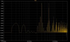
This “toy” amp sim shows this pretty unambiguously; the outputs are weakly class AB biased so the vas has plenty of work to do correcting distortion
To address objections to “resistive load” I’ve added a non-harmonic load current – you can see from the I-V plane plot that the output is being exercised over a more substantial region than any reactive load would cause
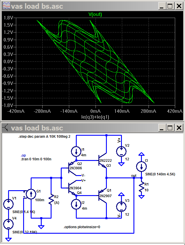
Again in the fft I’m just showing the distortion, 1 KHz 0dB and 19KHz -12 dB are off the fft plot
What you should see is that the prominent 4.5KHz peak from the output load current shows that output Z is uniformly degraded by heavier vas load – further the bright green 10K loaded vas trace shows the most harmonic and IMD distortion with any combination of input signal and load current
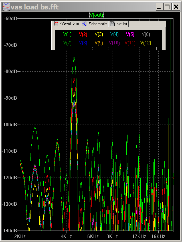
(2KHz left edge is 2nd harmonic of 1KHz input, peaks occur every 500 Hz moving right, for instance count peaks from the left edge 2.0KHz , 2.5KHz, 3KHz, ... and you can see that simple loop gain is reducing the 3rd harmonic as peak amplitude colors inversely follow the resistor load step color order from bright gren 10KOhm load increasing in 10^.5 steps)
The one “interesting”anomaly is the 2.5KHz third order distortion product (4.5KHz – 2* 1KHz) – this distortion seems to go through a minimum at 100Kohm load (yellow) and actually increases for higher vas load – so for some specific distortion mechanisms it is possible to find an optimum vas load, but you have a lot of work ahead of you to convince me that such specific optimization can be more attractive than the robust improvements across the board that high loop gain (no vas loading) gives
LtSpice cir file; change .txt to .asc
Vas load simply reduces loop gain and Increases output Z and distortion, including IMD, it is Not “equivalent to emitter degeneration in another place”
This “toy” amp sim shows this pretty unambiguously; the outputs are weakly class AB biased so the vas has plenty of work to do correcting distortion
To address objections to “resistive load” I’ve added a non-harmonic load current – you can see from the I-V plane plot that the output is being exercised over a more substantial region than any reactive load would cause
Again in the fft I’m just showing the distortion, 1 KHz 0dB and 19KHz -12 dB are off the fft plot
What you should see is that the prominent 4.5KHz peak from the output load current shows that output Z is uniformly degraded by heavier vas load – further the bright green 10K loaded vas trace shows the most harmonic and IMD distortion with any combination of input signal and load current
(2KHz left edge is 2nd harmonic of 1KHz input, peaks occur every 500 Hz moving right, for instance count peaks from the left edge 2.0KHz , 2.5KHz, 3KHz, ... and you can see that simple loop gain is reducing the 3rd harmonic as peak amplitude colors inversely follow the resistor load step color order from bright gren 10KOhm load increasing in 10^.5 steps)
The one “interesting”anomaly is the 2.5KHz third order distortion product (4.5KHz – 2* 1KHz) – this distortion seems to go through a minimum at 100Kohm load (yellow) and actually increases for higher vas load – so for some specific distortion mechanisms it is possible to find an optimum vas load, but you have a lot of work ahead of you to convince me that such specific optimization can be more attractive than the robust improvements across the board that high loop gain (no vas loading) gives
LtSpice cir file; change .txt to .asc
Attachments
Re: mike, be prepared to be disapointed...
Thanks jcx, i will do my best... 😉
Mike
jcx said:but you have a lot of work ahead of you to convince me that such specific optimization can be more attractive than the robust improvements across the board that high loop gain (no vas loading) gives
Thanks jcx, i will do my best... 😉
Mike
As said by JCX, a resistor in the collector of the Vas is not at all "equivalent to emitter degeneration in another place".
Sorry, such a misunderstanding can only makes to hardly contest your claims of perfection for your "symasym" amp?
See Self's writings about the effects on distorsion by resistive and capacitive loading of the Vas output.
A much nicer way to do things is to use a feedback resistor in parallel with the miller capacitor between the input and output of the VAS.
It allows to enhance open loop bandwith with a very little more distorsion. However my ears did not notice any audible gain in quality.
~~~~~~~~ Forr
§§§
Hi jcx,
I had a closer look to your toyamp, the only thing this schematic
demonstrates to me is the benefit of higher feedbackfactor.
Okay, i am not familiar with LTspice, but this G1 device looks like
a "perfect" amp without any weaknesses. Maybe you should at
least put a cap in paralell to this G1 to simulate the outputcapacitance
of the vastransistors ? Also you should add a real feedbacknetwork
to get correct behaviour of a feedbackloop.
Hi forr,
the only thing i definitely know is that the resistorloads made the
amp sound softer/cleaner, at a not subtile level.
Most of the symasym is not based on science then rather changing
and listening.
I am still at work, i will try to demonstrate some sims later...
Mike
Mike,
Loading the VAS resistively does a few things, chiefly:
1. Helps to cover over the cracks in the Class AB switching by more evenly loading the VAS.
2. Reduces the reflected reactance effects of the speaker for the same reason as #1 above.
3. Reduces OLG, bringing back feedback factor, increasing Zout and increasing distortion.
The increased Zout is of little importance as with GFB amps it is very low anyway. There is little sonic difference between a damping factor of 80 and 200.
Concerning distortion increases, you may be hearing the masking effect of increased lower order distortion, which covers over the more objectionable high order distortion. This is clearly a balancing act. The acid test would be very complex, orchestral music at high volume, where IMD is almost always evident.
JCX's plots do not reveal why precisely your amp sounds better with stiff resistive loading of the VAS. I believe the reason is psychoacoustic.
Cheers,
Hugh
Here it comes !
Hi !
Here are some sim-results about the difference between vasloading
and using re's. I used the circuit from symasym, it's possible that
things are slightly different here than in a normal pushpull-vas,
but i had not too much time, and the pushpullvas showed only gain
of 1:20 which was not too representive...
These sims are only openloop for now.
Here are the 2 schematics i used:
emitter-resistors:
vasloaded:
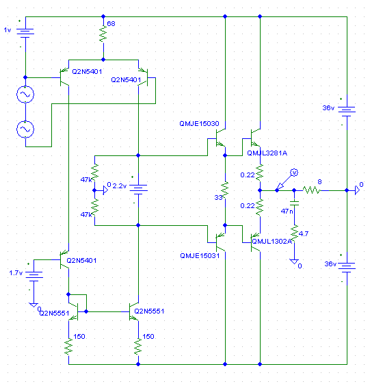
Both circuit are set to the same gain, 1:1350, here is the acsweep
showing the gain for 10mv input:
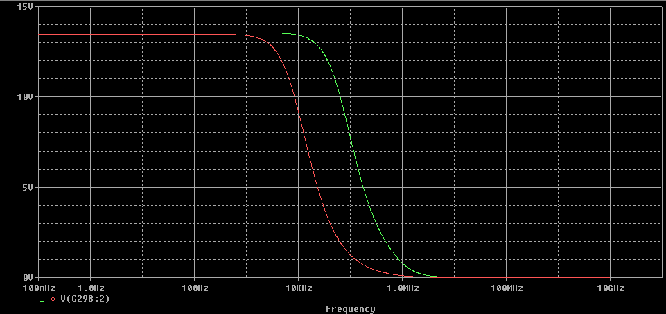
Red = Re's / Green = loadedvas
And the distortionfigures: (same colors)
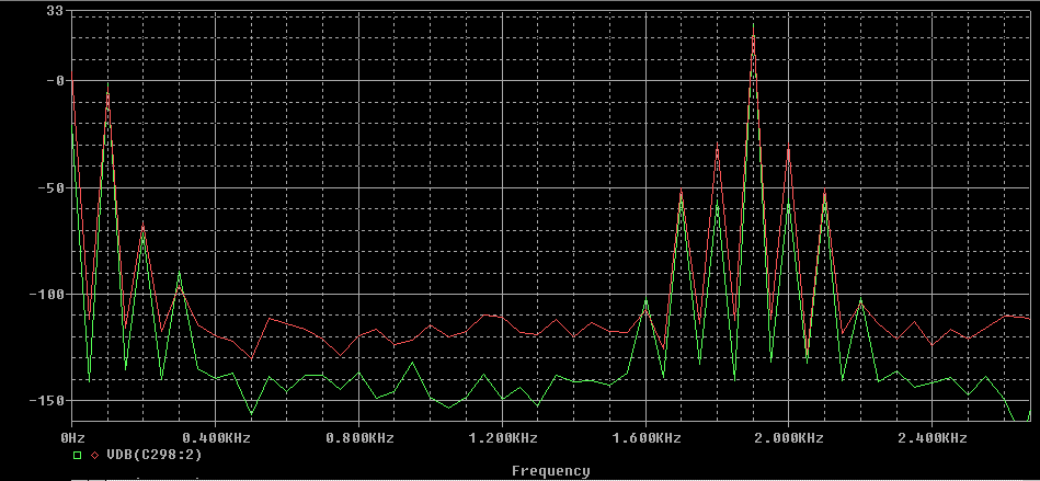
I had to use very low freqs for IMD-test, re-version was simply too slow !
(0.1khz,0.7mv + 1.9khz 16mv)
Hugh, you forgot No4, increased OLBW...
No further comment except i hope that i have not done any dumb mistake...
Mike
Hi !
Here are some sim-results about the difference between vasloading
and using re's. I used the circuit from symasym, it's possible that
things are slightly different here than in a normal pushpull-vas,
but i had not too much time, and the pushpullvas showed only gain
of 1:20 which was not too representive...
These sims are only openloop for now.
Here are the 2 schematics i used:
emitter-resistors:
vasloaded:
Both circuit are set to the same gain, 1:1350, here is the acsweep
showing the gain for 10mv input:
Red = Re's / Green = loadedvas
And the distortionfigures: (same colors)
I had to use very low freqs for IMD-test, re-version was simply too slow !
(0.1khz,0.7mv + 1.9khz 16mv)
Hugh, you forgot No4, increased OLBW...
No further comment except i hope that i have not done any dumb mistake...
Mike
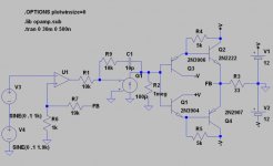
MikeB
Here's a circuit (mostly 'ideal' components to analyse the effects of VAS output impedance.
U1 is a gain of 10 10MHz BW amp, G1 may be considered a perfect transistor (a transconductance - the transistor's gm = 1/re). It's output impedance is infinite, so at lower freq the stage output impedance is equal to R2.
R9/C1 stabilizes the loop, it's effects are minor up to 10kHz, but significant from some 100kHz on.
Let's start with R2=1meg and G1=100uA/V for a gain of 100; then let's reduce R2 to 100K and increase G1 to 1mA/V for the same gain of 100, and so on.
This way, one can separate the effects of VAS output impedance from feedback (since feedback is constant) and open loop linearity (your Re in or out would change open loop linearity).
Attachments
- Status
- Not open for further replies.
- Home
- Amplifiers
- Solid State
- Feedback delay & distortion