Save your 546a or 546b to use when you need their 60Vce0
buy some high gain low noise bc549c or 550c & 559c or 560c for when they are needed.
Buy some cheap 2n5551 and 2n5401 for their 160Vce0 with reasonable fT and hFE and 500mA.
It's rare that you would need them, but mpsa42/92 are good to 300Vce, but that HV capability compromises their hFE and their fT, so they don't make good general purpose devices.
BTW,
I like using a regulator to feed a relay timing circuit. It brings most of the advantages of the proper timer and gives a lot more flexibility than comes with a 555 timer chip.
You could go to even higher voltage, maybe to 30V, or even 36V, to drive your 24V relay/s (or two 12V relays in series). Then adopt a current saving circuit to allow the relay to run cool.
buy some high gain low noise bc549c or 550c & 559c or 560c for when they are needed.
Buy some cheap 2n5551 and 2n5401 for their 160Vce0 with reasonable fT and hFE and 500mA.
It's rare that you would need them, but mpsa42/92 are good to 300Vce, but that HV capability compromises their hFE and their fT, so they don't make good general purpose devices.
shows the wide range of suitable transistors for a relay driver.in the PDF is listed that I can use 550C 2N5551
BTW,
I like using a regulator to feed a relay timing circuit. It brings most of the advantages of the proper timer and gives a lot more flexibility than comes with a 555 timer chip.
You could go to even higher voltage, maybe to 30V, or even 36V, to drive your 24V relay/s (or two 12V relays in series). Then adopt a current saving circuit to allow the relay to run cool.
Last edited:
Save your 546a or 546b to use when you need their 60Vce0
buy some high gain low noise bc549c or 550c & 559c or 560c for when they are needed.
Buy some cheap 2n5551 and 2n5401 for their 160Vce0 with reasonable fT and hFE and 500mA.
It's rare that you would need them, but mpsa42/92 are good to 300Vce, but that HV capability compromises their hFE and their fT, so they don't make good general purpose devices.shows the wide range of suitable transistors for a relay driver.
BTW,
I like using a regulator to feed a relay timing circuit. It brings most of the advantages of the proper timer and gives a lot more flexibility than comes with a 555 timer chip.
You could go to even higher voltage, maybe to 30V, or even 36V, to drive your 24V relay/s (or two 12V relays in series). Then adopt a current saving circuit to allow the relay to run cool.
So I should use 550C's for the Input stage (Q1,Q2) instead of the 546b's ?
Hi Mace,
Use the transistors with the least noise and highest measured gain. You need to match these and the amp you are building will respond very well to this. I've made a few and really like them a lot. With some effort put in now, these amps may well last you decades of being your best amplifier. They are better than the average amplifier out there.
-Chris
The relay driver does not need low noise, nor very high gain transistors. 2n5551 would do. If the charge current passing to C26 is very low then the base current into Q13 also needs to be very low.So I should use 550C's for the Input stage (Q1,Q2) instead of the 546b's ?
Q14 should run saturated (Ib~10% of Ie)
Q1 & 2 are not shown.
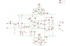
Are you referring to post4015 pic ?
It has jFETs at the input
Last edited:
The relay driver does not need low noise, nor very high gain transistors. 2n5551 would do. If the charge current passing to C26 is very low then the base current into Q13 also needs to be very low.
Q14 should run saturated (Ib~10% of Ie)
Q1 & 2 are not shown.
Are you referring to post4015 pic ?
It has jFETs at the input
Hey anatech, yeah okay then I buy some of the BC550C's, I think it's a good investment 😎
Oh Yeah sorry, I marked them in these Screenshots... Then you can see the green Square with the BD139 ? I Have some BD179 here from my spareparts but not the 139's can I use them too ?
Sorry for that much questions but I have so much complementary types here 😀
PS: How do I solder the R38 in ? Pin 1 and 3 with 480KOhm's ?
Last edited:
Hi Mace,
I'll let Andrew deal with that question about the BD numbers. I would have to look each on up because I don't use them normally. Its an "other side of the pond" thing. 🙂
-Chris
I'll let Andrew deal with that question about the BD numbers. I would have to look each on up because I don't use them normally. Its an "other side of the pond" thing. 🙂
-Chris
Hi Mace,
I'll let Andrew deal with that question about the BD numbers. I would have to look each on up because I don't use them normally. Its an "other side of the pond" thing. 🙂
-Chris
Haha okay 😀
Onsemi show quite a bit of data for the bd179.
Gain falls a lot at lower and higher Ie.
They even warn that base emitter dissipation prevents continuous use around 2A and yet it is specified as a 3A device. It's OK if you keep Ie between 5mA and 200mA
fT=3MHz,
0.54A Ie @ 40Vce
I would not use it.
Gain falls a lot at lower and higher Ie.
They even warn that base emitter dissipation prevents continuous use around 2A and yet it is specified as a 3A device. It's OK if you keep Ie between 5mA and 200mA
fT=3MHz,
0.54A Ie @ 40Vce
I would not use it.
Onsemi show quite a bit of data for the bd179.
Gain falls a lot at lower and higher Ie.
They even warn that base emitter dissipation prevents continuous use around 2A and yet it is specified as a 3A device. It's OK if you keep Ie between 5mA and 200mA
fT=3MHz,
0.54A Ie @ 40Vce
I would not use it.
Okay then I will buy some new BD139's and some BC550C's for the inputstage.
🙂
Well then I have a question about the heatsinks, I have a Alumunimum Heatsink with 0,9K/W here, is this sufficient for cooling my Powertransistors ? And can I mount the Transistors with short cables ? Because the Heatsink is not wide enough to support the whole PCB to mount it directly on the heatsink.
I would mount them like in the picture.
Attachments

Last edited:
You can use modelling to help predict temperatures.
The 3886 datasheet is quite good. National give the formula to predict the maximum power dissipation to the sink using just |Vcc|+|Vee| and Rload.
They, as usual, forget to mention that reactive loads are a worse case. ESP explains this fairly well.
The 3886 datasheet is quite good. National give the formula to predict the maximum power dissipation to the sink using just |Vcc|+|Vee| and Rload.
They, as usual, forget to mention that reactive loads are a worse case. ESP explains this fairly well.
Last edited:
The size of the PCB is 210 x 94mm. A heatsink with a height of 100mm is sufficient therefore.
Make sure that your heatsink is long enough to screw the output transistors, drivers and BD139 (used in the temperature compensation circuit) directy to the heatsink.
Do not connect the output transistors via cables to the PCB. Screw them to the heatsink (tap the heatsink) beneath the PCB at the specified posistions.
Concerning the heatsink's temperature properties: if you play the SYMASYM at 30VA (which is very loud in my ears) and you have an ambient temperature of about 25°C,
the SYMASYM will add about 30 x 0.9°C to the heatsink resulting in a total of about 52°C - which is tolerable in my eyes. (This is a very rough formula though!).
If you leave the jumper of the onboard-multiplier open (as shown on your image), the SYMASYM's frontend-voltage is clamped to about 36VDC by the used Zener diode D3.
Best regards - Rudi_Ratlos
The size of the PCB is 210 x 94mm. A heatsink with a height of 100mm is sufficient therefore.
Make sure that your heatsink is long enough to screw the output transistors, drivers and BD139 (used in the temperature compensation circuit) directy to the heatsink.
Do not connect the output transistors via cables to the PCB. Screw them to the heatsink (tap the heatsink) beneath the PCB at the specified posistions.
Concerning the heatsink's temperature properties: if you play the SYMASYM at 30VA (which is very loud in my ears) and you have an ambient temperature of about 25°C,
the SYMASYM will add about 30 x 0.9°C to the heatsink resulting in a total of about 52°C - which is tolerable in my eyes. (This is a very rough formula though!).
If you leave the jumper of the onboard-multiplier open (as shown on your image), the SYMASYM's frontend-voltage is clamped to about 36VDC by the used Zener diode D3.
Best regards - Rudi_Ratlos
Alright, thanks Rudi !
Hello guys,
I hope you can help me. I cant bias one of my two Black-Beauties. I already changed all of the small transistors, because one of them (Q5/6/7) was defect and "opened" the output stage.
Now I cant bias the amp. Between MP1 and MP2 are 0,000VDC and this value doesnt change when i turn R18. I also meassured around 0,1VDC between Speaker-Out and ground.
I hope you can help me.
Sven
P.S.: I also changed the BD139. This reduced the voltage between Speaker-Out and ground (0,5V-->0,1V)
Attachments
measure across C12 or across Q11 when adjusting the bias voltage.
You see the change immediately.
If you clip on a multi-meter here AND also across R26+R25, you can monitor BOTH voltages as you adjust.
You see the change immediately.
If you clip on a multi-meter here AND also across R26+R25, you can monitor BOTH voltages as you adjust.
The voltage drop across Q11 is 0,03V if R18 is 500 Oh and 0,025V if R18 is 0 Ohm.
The voltage drop of the working channel is about 2,4V.
The voltage drop of the working channel is about 2,4V.
It's cool if you have a working channel! You just have to compare the measurements to locate the error.
Start with the operating points: for example check the voltage on R8, R9, R10, R11, R12.
If the trimmer and Q11 are OK then the problem is probably somewhere "earlier".
Start with the operating points: for example check the voltage on R8, R9, R10, R11, R12.
If the trimmer and Q11 are OK then the problem is probably somewhere "earlier".
Working/Defect
R8: 0,98V/0,12V
R9: 0,97V/0,66V
R10: 0,36V/0,12V
R11: 0,37V/0,003V
R12: 0,39V/0,003V
R8: 0,98V/0,12V
R9: 0,97V/0,66V
R10: 0,36V/0,12V
R11: 0,37V/0,003V
R12: 0,39V/0,003V
Cool, thanks! As it seems there's already something wrong around the LTP.
Check every part around Q1, Q2, Q3, Q4! The tarnsistors with the diode
method (DMM "+" to the base, DMM "-" first to emitter and then to the collector:
correct values should be around 6-700...) And then measure all the resistors
as well, compare with the other channel as well. That's all for 1st step... 😉
- Home
- Amplifiers
- Solid State
- Explendid amplifier designed by Michael Bittner, our MikeB