variations on EZ mos
Of course I had to mess with this. BTW, thanx for posting a functional spice file!
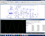
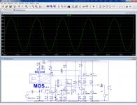
1. Move R10 (and adjust) so that you get more feedback and you get about 20% lower distortion (0.6% -> 0.5%).
2. Adding another gain stage is a bit tricky because the Vto of the MOS VAS is so high, so you have to reduce the drop on the feedback resistor by reducing them. But the result is about 0.04% THD.
3. Since we have only single pair of output devices, the source resistors are optional and if you remove them you get about 0.02% THD.
4. But the bias current runs a bit hot so tweaking it down from 180mA to about 32mA will cool things off and only raises THD to 0.03%, still not bad.
BTW, I moved Vout to the other side of the cap. I would do single supply differently but then it's not the same amp at all.
Thanx again.
SteveU
Of course I had to mess with this. BTW, thanx for posting a functional spice file!
1. Move R10 (and adjust) so that you get more feedback and you get about 20% lower distortion (0.6% -> 0.5%).
2. Adding another gain stage is a bit tricky because the Vto of the MOS VAS is so high, so you have to reduce the drop on the feedback resistor by reducing them. But the result is about 0.04% THD.
3. Since we have only single pair of output devices, the source resistors are optional and if you remove them you get about 0.02% THD.
4. But the bias current runs a bit hot so tweaking it down from 180mA to about 32mA will cool things off and only raises THD to 0.03%, still not bad.
BTW, I moved Vout to the other side of the cap. I would do single supply differently but then it's not the same amp at all.
Thanx again.
SteveU
Attachments
Sorry for getting ahead of me, I thought it was a final version and it would be of somebody's interest to pcb.
Don't be sorry: many people will probably prefer to build the plain vanilla version for some reason or another.
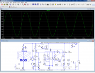
It should work alright for all practical purposes, but the figures don't particularly shine, which is generally not a problem unless you attention is solely focused on the test instruments instead of the program (I am currently listening to Bide & Musique through a Dell/Altec Lansing system, to put things in perpective)
It should work alright for all practical purposes, but the figures don't particularly shine, which is generally not a problem unless you attention is solely focused on the test instruments instead of the program (I am currently listening to Bide & Musique through a Dell/Altec Lansing system, to put things in perpective)
Attachments

The additional input transistor is already the current configuration for the high power version, but the resistors values are more realistic, in particular R15.2. Adding another gain stage is a bit tricky because the Vto of the MOS VAS is so high, so you have to reduce the drop on the feedback resistor by reducing them. But the result is about 0.04% THD.
470K will cause a huge HF rolloff in combination with the MOS capacitances, and it will also severely limit the the slewrate.
With vertical MOSFets, the source resistors are not really optional: it might appear to work in sim, and for static conditions in reality, but as soon as a thermal excursion occurs, it will go into thermal runaway.3. Since we have only single pair of output devices, the source resistors are optional and if you remove them you get about 0.02% THD.
4. But the bias current runs a bit hot so tweaking it down from 180mA to about 32mA will cool things off and only raises THD to 0.03%, still not bad.
With LatFets, the situation would be very different.
In addition, it would be impossible to implement the auto-bias feature
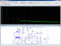
Here is the anti-thump circuit implemented with a cap-multiplier:
I am still undecided about the final choice
Attachments
You could also shunt the R18 with a diode; to "get down" real quick on turn-off. Otherwise it may "pop" on quick turn-on/turn-off/turn-on.
Do you realize you just made a deluxe version of the amp? With "polished" input/vas rail ... that's "almost audiophile" touch! (crude, rude&elegant)
Do you realize you just made a deluxe version of the amp? With "polished" input/vas rail ... that's "almost audiophile" touch! (crude, rude&elegant)
Here is the full-option circuit, in its (hopefully) definitive version:
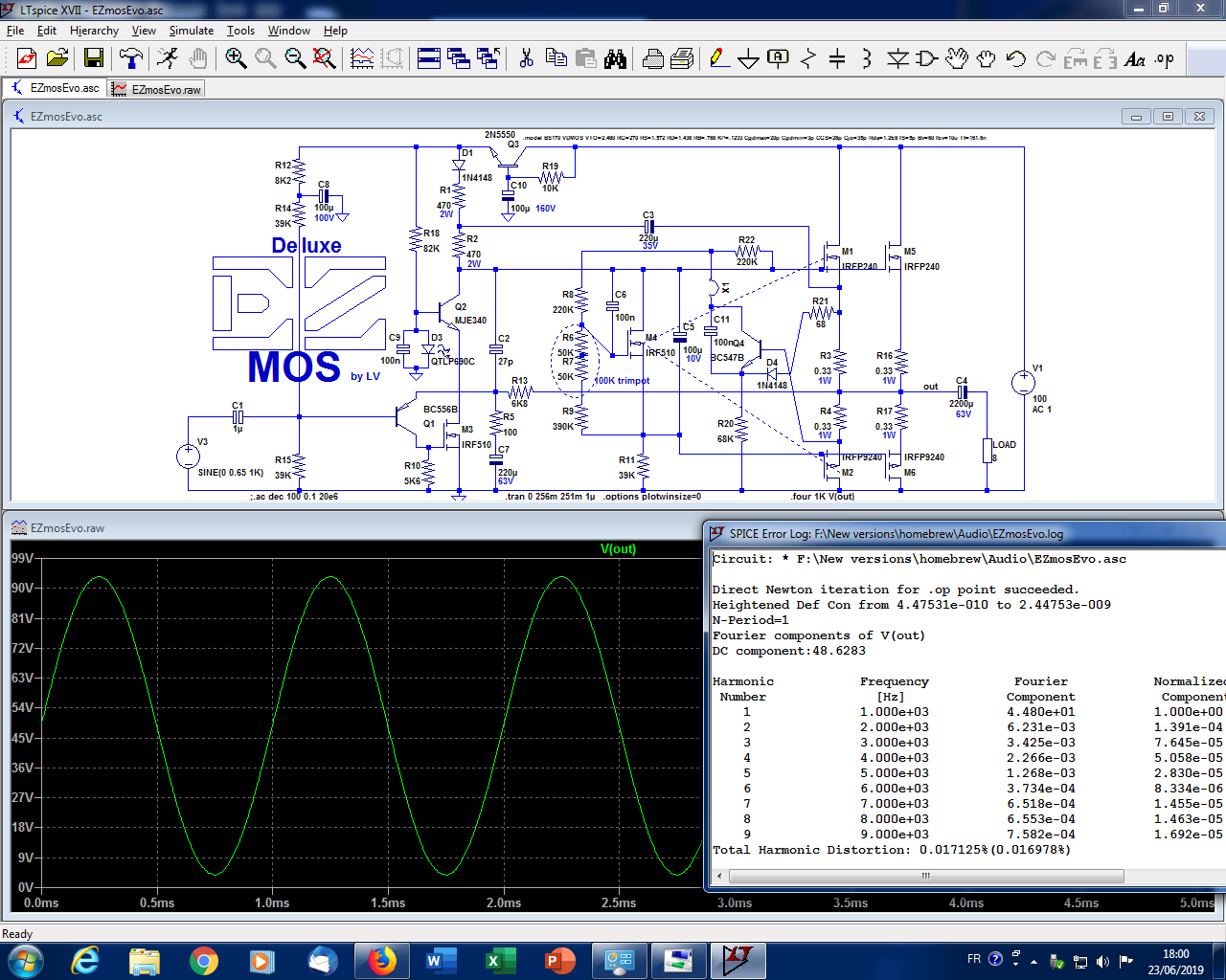
The THD level is acceptable, and could probably be tweaked, but it makes little sense to do it in sim: the reality could be somewhat different.
If an option is not required, the corresponding components can be just omitted, and the C-E space replaced by a strap.
With the cascoded version, the IRF510 is not necessary anymore, and could be replaced by BS170; performances would be somewhat better.
The cascode transistor will dissipate ~2.5W, and needs a heatsink.
For these reasons, it would be helpful if the PCB is made to accept both TO220 and TO92.
An important reminder: this circuit has not been tested in reality.
Note that the supply voltage of the example is 100V, but it could range from 30 to 100V without a single modification.
Supplies higher than 100V are also possible, but it will be necessary to increase the ratings of the Ecaps and power resistors.
Attachments
Too late to edit, but I just realized I forgot to draw the fuse and general bypass cap on the scematic
If supply higher than 100V; perhaps the cap-multi should be a TO-220 mosfet (with that damn diode across R19) and R-C scaled at cca. factor 10 (10u/100k).
What about power-mosfet gate stoppers?
What about power-mosfet gate stoppers?
Yes, that is something I considered, because it allows a much smaller cap, but the Vto will eat up a few volts of gate drive to the OP's, and I want to keep the design extra-efficient.If supply higher than 100V; perhaps the cap-multi should be a TO-220 mosfet (with that damn diode across R19) and R-C scaled at cca. factor 10 (10u/100k).
That said, the diode-augmented bootstrap could be sufficient to erase the additional voltage loss; that is something I am going to test, because a 100µ/160V is somewhat bulky (and it is the absolute minimum possible here)
I generally try to avoid them whenever possible: they may improve local stability, but they increase the HF phaseshift of the GNFB, not something desirable.What about power-mosfet gate stoppers?
Here, the gate drive of the MOSFets acts more or less as a gate stopper, if the layout is compact enough (my build does not use any and is perfectly stable).
Were they are driven from followers, the situation would be quite different.
However, with paralleled devices, different "modal" oscillations can also occur (ie. the pair operating as a push-pull oscillator), but the source resistors tend to damp things down.
Thiagomogi's PCB already includes a provision for stoppers, and it does no harm to keep all the options open: resistor, strap or ferrite bead.
In the same vein, adding 15V zeners across the G-S of the Fets came sometimes save the day when things really go sour (like a source resistor failing open)
Here is an updated version: the circuit tolerates the additional drop without limiting the output swing.
The MOSFet does not necessarily need to be a TO220: the permanent dissipation is very low, and the transient power is relatively limited because the load is essentially resistive.
A BSP89 or equivalent would be perfectly sufficient.
With other components values and diodes omitted, the circuit remains compatible with a BJT.
I have also refined some components values, and added the fuse and a general bypass cap
Attachments
Minor nitpick: R12/R14/C8. How about change to 12K/33K and reuse 47uF/160V in this position?
Or 18K/27K (to unify the BOM).
Perhaps C3 could be made same as C7 as well. (I mean for builders if that's intended as a project?)
Or 18K/27K (to unify the BOM).
Perhaps C3 could be made same as C7 as well. (I mean for builders if that's intended as a project?)
Sensible alternatives for sure, but would-be builders now have sufficient information to decide by themselves, and the 100V example is just that: an example.
The components ratings are minimal for this example, but if people decide to build a 70V or 140V version, or use higher voltage caps, for availability or other reasons, they are free to do so.
If a doubt remains, any question can be posted in this thread and will be adequately answered (however, I remind once again that the high-power, Evo version has not (yet) been tested in reality)
Last edited:
If a doubt remains, any question can be posted in this thread and will be adequately answered (however, I remind once again that the high-power, Evo version has not (yet) been tested in reality)
Elvee, since this is 'old school' kind of amp, I was wondering if quasi
output devices could be easily implemented (like in your circlophone)?
I guess one extra transistor would be needed, right?
Elvee, since this is 'old school' kind of amp, I was wondering if quasi
output devices could be easily implemented (like in your circlophone)?
I guess one extra transistor would be needed, right?
I'm dying to see what LV comes up with for a quasi circuit. Two possibilities are:
1. Use the lower power FET as the VAS with a diode in the drain.
2. Offset the ~PNP/P-channel driver bias above the output, perhaps at the upper n-fet gate voltage.
I have played with both these and more but unless you need to put it all on a single n-channel die, there is no point. I could dig up the some simulations if anyone cares.
It could look like this (not for construction, just a concept):Elvee, since this is 'old school' kind of amp, I was wondering if quasi
output devices could be easily implemented (like in your circlophone)?
I guess one extra transistor would be needed, right?
Another possibility is a CircloMos converted to a single supply (easily done):
https://www.diyaudio.com/forums/solid-state/154388-cheap-dirty-circlomos.html?highlight=circlomos
Attachments
What happened to temp sensing and bias pot?It could look like this (not for construction, just a concept)
Gone for good, or just because it's a 'concept'?
How is the bias between the gates of output devices set/maintained?
Last edited:
- Home
- Amplifiers
- Solid State
- Easy-MOS is a simplistic, efficient and evolutive all-MOS amplifier for beginners