The leakage inductance shouldn't matter at amp impedances. Luckily only the leakage capacitance may have an effect on audio response, if the trafo is obscenely large.
hi
really considering building one of these - great work all round 🙂 as ive mentioned in other threads I currently use a self trimodal design. bought some huge martin logan speakers last week and the tri isn't really cut out for driving them. was considering building myself another load invariant but having tried two of dougs designs (with huge success) perhaps its time for something else. it seems only right !
just been trawling my stores (ie huge plastic box full of components) and have found some devices that may be suitable so just wanted to check (having just moved house and blown last pennies on speakers i need to build this as cheaply as possible) if i could use these devices ...
i have 6 MJL4281AG and 6 MJL4302AG for output devices, and enough MJE15034/5 G to use for drivers.
would these be suitable?
I also am wondering what supply rail would be best. The speakers are 4r but apparently dip to 1.2r at 20Khz. They are rated to 200W.
Advice welcome
Thanks folks
Yes.hi
i have 6 MJL4281AG and 6 MJL4302AG for output devices, and enough MJE15034/5 G to use for drivers.
would these be suitable?
With speakers 4R and below to be on the safe side I'd stay around and below 45V to not exceed the trannies' SOA. This should give you enough op power.I also am wondering what supply rail would be best. The speakers are 4r but apparently dip to 1.2r at 20Khz. They are rated to 200W.
BR,
Holgi
Yes.
With speakers 4R and below to be on the safe side I'd stay around and below 45V to not exceed the trannies' SOA. This should give you enough op power.
BR,
Holgi
Thanks for the reply Holgi. Good news. I think I have suitable power supply transformer for those rails - I have a large screened toroidal with 33-0-33. So should give me about 45V rails.
Time to order some pcbs !
Thanks
Gerber
Hi,
Does anyone have a gerber file for the honey badger of OS 's design, I'm lucky enough to have access to a milling machine of my brothers, I don't really fancy I/p all those components into an auto router....
Btw fantastic reading these design pages...
Cheers
Mike
Hi,
Does anyone have a gerber file for the honey badger of OS 's design, I'm lucky enough to have access to a milling machine of my brothers, I don't really fancy I/p all those components into an auto router....
Btw fantastic reading these design pages...
Cheers
Mike
The Honey Badger is a design that was commissioned by DIYaudio for inclusion in DIYaudio's retail arm.
Honey Badger belongs to DIYaudio.
You need to ask DIYaudio if they are willing to send you their IP (unless there is an agreement with OST that he retains the IP) and to take the risk of you not selling on the Gerbers to other manufacturers.
Honey Badger belongs to DIYaudio.
You need to ask DIYaudio if they are willing to send you their IP (unless there is an agreement with OST that he retains the IP) and to take the risk of you not selling on the Gerbers to other manufacturers.
Gerber
Ah, I see, thx for that, I can see the whole rip off problem..
Pity really that people find it necessary...
Guess I'll have to find a light box.
Mike
Ah, I see, thx for that, I can see the whole rip off problem..
Pity really that people find it necessary...
Guess I'll have to find a light box.
Mike
Yes , the layout was posted since the initial design phase. You could do the
toner transfer method.
The gerber's are only for DIYA use !
OS
toner transfer method.
The gerber's are only for DIYA use !
OS
Hi Guys,
Well I finished populating the boards and got them mounted on some heat sinks so I wanted to test them out. I don't have the power supply that I will be using with it set up yet so I hooked it up to the PS that I put together for a VSSA which is a 25-0-25VAC 600VA Antek transformer and a Mr Evil Capacitance Multiplier. This is putting out about +/-39VDC. So I hooked up the first board and brought it up nice and slow on my variac with a light bulb in line and 10R 1W resistors in place of the fuses. Everything looked good so I set the front end, adjusted the offset to 00.1mv and brought up the bias to 20mV across TP1 and TP2. Nice, looks good. So I hook up the second board and bring it up and not so good. Can't adjust the bias, can't adjust the offset. Front end looks OK. Great! Now what. So I hook up both boards side by side and start comparing. the voltages are all wrong on the drivers and bias transistors. Turns out, the jumpers that run across to the drivers have no continuity. I'm thinking maybe I just didn't get the solder mask scraped off well enough so I scraped them some more. No way, the jumper isn't connected so I just run a wire across under the board for both jumpers and problem solved. Now both boards measure the same and I can set the off set and bias, no problem. Now I'm feeling pretty good so I decide to see how it looks on a scope. I hook up the scope and with no load attached I run a sine wave through it. Now I see another problem. I get about half way up with the sine wave generator and I see the wave start clipping and the top wave has what looks like oscillation. I think maybe adding a load will help but no. I hook up an 8R dummy load and I'm still seeing the weird little oscillation on the top of the wave. The bottom is clipping but is just flat. So I hook up the other channel to the input so I can compare the waves an I see a little fuzz at the top of the input sine wave. I unhook the generator and check it and the fuzz isn't there. Only when it is hooked to the amp so that fuzz is somehow coming from the input on the amp and it is only on the top part of the wave, not the bottom.
By the way, I measured the output and it is putting out about 25VAC at the point of clipping with the 8R load attached. Both channels are acting the same.
Any ideas? have any of you guys experienced anything similar?
Thanks, Terry
Terry:
Try just working on ONE board at a time. Get one working, then the other one will be a piece of cake.
Good luck and be careful...
Try just working on ONE board at a time. Get one working, then the other one will be a piece of cake.
Good luck and be careful...
Thanks for responding, They are both doing the same thing. I'm all for getting on working first. Any ideas why it is doing what it is doing?
Tamed the clipping !!
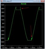
Member Still4given hard clipped his Badger ...
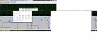
The result was a slight sticking of the upper rail waveform (pix 1).
The simulator emulated exactly the result on the actual amp (build thread)
by still4given (so I trust it - the models). You can also see a little burst of oscillation induced by the hard clip (arrows - pix 1).
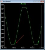
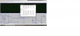
Member Janutz (thanks!!) recommended a diode from the collector of Q10 to
the base of Q9 - It works (according to the simulation - pix 2).
Still , a little burst of oscillation. 🙁🙁 Some diode models worked with R18=820R,
some showed the little burst. The speed of the diode seems to determine this ??
This little burst does not happen with standard miller compensation. So, it has to be TMC's fault... 😀
I lowered the TMC feedback resistor to R18=1.5k ... burst is gone - even with a slow garbage diode.
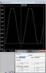
The final (pix 3) , shows almost perfect symmetrical clipping (within .5V) AND no
bursts or other errata. I ran this with many rail voltages and with different gains.
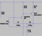
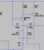
Attachment 4 shows the Badger VAS (Q9/10) with the added diode (D3).
This diode should be both fast and have a high reverse breakdown voltage
as it has to see the full "swing" of the VAS verses the relative static voltage
present at the base of Q9.
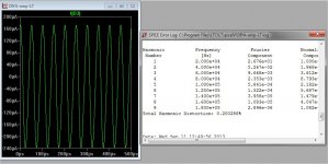
The effect of raising the value of R18 was just a 5 PPM distortion increase at 20K ! WORTH it!
SO , in conclusion R18 is just a value change and D3 would be very easy
to add either to the top or bottom of the PCB - no major rework.
OS
Member Still4given hard clipped his Badger ...
The result was a slight sticking of the upper rail waveform (pix 1).
The simulator emulated exactly the result on the actual amp (build thread)
by still4given (so I trust it - the models). You can also see a little burst of oscillation induced by the hard clip (arrows - pix 1).
Member Janutz (thanks!!) recommended a diode from the collector of Q10 to
the base of Q9 - It works (according to the simulation - pix 2).
Still , a little burst of oscillation. 🙁🙁 Some diode models worked with R18=820R,
some showed the little burst. The speed of the diode seems to determine this ??
This little burst does not happen with standard miller compensation. So, it has to be TMC's fault... 😀
I lowered the TMC feedback resistor to R18=1.5k ... burst is gone - even with a slow garbage diode.
The final (pix 3) , shows almost perfect symmetrical clipping (within .5V) AND no
bursts or other errata. I ran this with many rail voltages and with different gains.
Attachment 4 shows the Badger VAS (Q9/10) with the added diode (D3).
This diode should be both fast and have a high reverse breakdown voltage
as it has to see the full "swing" of the VAS verses the relative static voltage
present at the base of Q9.
The effect of raising the value of R18 was just a 5 PPM distortion increase at 20K ! WORTH it!
SO , in conclusion R18 is just a value change and D3 would be very easy
to add either to the top or bottom of the PCB - no major rework.
OS
Attachments
Last edited:
Member Still4given hard clipped his Badger ...
The result was a slight sticking of the upper rail waveform (pix 1).
The simulator emulated exactly the result on the actual amp (build thread)
by still4given (so I trust it - the models). You can also see a little burst of oscillation induced by the hard clip (arrows - pix 1).
Member Janutz (thanks!!) recommended a diode from the collector of Q10 to
the base of Q9 - It works (according to the simulation - pix 2).
Still , a little burst of oscillation. 🙁🙁 Some diode models worked with R18=820R,
some showed the little burst. The speed of the diode seems to determine this ??
This little burst does not happen with standard miller compensation. So, it has to be TMC's fault... 😀
I lowered the TMC feedback resistor to R18=1.5k ... burst is gone - even with a slow garbage diode.
The final (pix 3) , shows almost perfect symmetrical clipping (within .5V) AND no
bursts or other errata. I ran this with many rail voltages and with different gains.
Attachment 4 shows the Badger VAS (Q9/10) with the added diode (D3).
This diode should be both fast and have a high reverse breakdown voltage
as it has to see the full "swing" of the VAS verses the relative static voltage
present at the base of Q9.
The effect of raising the value of R18 was just a 5 PPM distortion increase at 20K ! WORTH it!
SO , in conclusion R18 is just a value change and D3 would be very easy
to add either to the top or bottom of the PCB - no major rework.
OS
Just simulated distorion with that extra diode from q10- q9. The distortion level increases 100 fold when using the diode.
Regards
Simon
Attachments
I know you say that with a wink, but seriously... If you intend to build one of these with high rail voltage > +-70v, and you never intend to play it at unreasonably high volume levels (no clipping), then would you necessarily need to worry about it? In affect, it would never rear its ugly head? Adding the extra, 2 component fix seems to be the answer and makes sense on a new build, but even with that solution you add distortion, so either way, even if you clip distortion will be added. Is that a correct conclusion? I guess distortion is better than clipping? 😀Just don't clip. 😉
Rick
p.s. @OS, I presume the amp can be built as is, and operated safely using >70vdc rails even though it has been optimized/designed for a max of 65v?
Last edited:
p.s. @OS, I presume the amp can be built as is, and operated safely using >70vdc rails even though it has been optimized/designed for a max of 65v?
Build it "as is" for 70V , my badger's supply is split. LTP/VAS run at 70Vdc ,output stage runs on 60Vdc. NO ISSUES !
Of the 2 errata I saw on still4givens scope , the burst (oscillation) is the worst. 😀
This can be eliminated simply by lowering TMC feedback , as I said this just raises THD20 by mere PPM.
On to.... this 😛 😛
By niss-man -Just simulated distorion with that extra diode from q10- q9. The distortion level increases 100 fold when using the diode.
I wondered (could not see the attachments too well) how he could of reached this conclusion.
Not all diodes (models) are created equal ... In [attachment 1] , we have a 1n5187 schottky. It's model shows 100's of uA reverse leakage equating to
that 100 fold increase in THD. A really bad form of local feedback.
NFB can't hope to compensate for this large of an error being fed back to the base of Q9. 🙁
I actually did my THD assessment using the "garbage" diode [attachment 2-1n4148] .. for a worst case scenario .so I thought... (MY ERROR 😱😱).
Still , we have 3 uA reverse leakage. However the Badger's NFB can compensate , giving .002% THD20 verses .0015% with no diode (8R load).
Now we know the mechanism for Niss's findings.
The Ideal diode SHOULD do absolutely NOTHING (like it is not there),until a saturation (clipping event) needs to be dealt with.
Looking around the web , I see that some diodes are WAY better in the reverse leakage category...
http://www.nxp.com/documents/data_sheet/BAS45A.pdf
Nice ! Only 1 NANO amp leakage. Only 125V reverse breakdown. 🙁
Another .. higher voltage..
http://www.diodes.com/datasheets/ds30371.pdf
100nA leakage , not too bad. That is 1/30th that of the 1n4148.
In conclusion , if the diode you use has ultra low leakage, it essentially
is "not there" under normal operating conditions.
Time to hunt down one of these "super diode" models for spice.
OS
Attachments

Last edited:
Here's a model...
http://www.vishay.com/docs/85252/bav21.txt
This one shows a realistic 600nA reverse current in simulation.
It reduces (some) "sticking" but does not add any distortion under normal
operation.
I think we need a faster diode , low reverse leakage , high reverse V.
Any suggestions ?
OS
http://www.vishay.com/docs/85252/bav21.txt
This one shows a realistic 600nA reverse current in simulation.
It reduces (some) "sticking" but does not add any distortion under normal
operation.
I think we need a faster diode , low reverse leakage , high reverse V.
Any suggestions ?
OS
Bring the diode to Q9's collector instead. The diode will turn on shortly before clipping, but until Q9's CB saturates, the increase in distortion will be minimal. Increase Q9's collector resistor too.
I tried it.Bring the diode to Q9's collector instead. The diode will turn on shortly before clipping, but until Q9's CB saturates, the increase in distortion will be minimal. Increase Q9's collector resistor too.
Your right about the THD.
But , the amp clips very asymmetrically and even shows a DC offset.
I used the BAV21 model , up to 1K for Q9's collector Resistor.
OS
Attachments

- Home
- Amplifiers
- Solid State
- diyAB Amp - The "Honey Badger"