I have noticed that the virtual ground circuit (C4, C5, R11, R12) can be is "noisy" when either V+ or V- is used as the ground reference and there is significant power supply ripple. For example, either of the PFET or NFET based mu follower follower (MUFF) output stages have very good power supply rejection ratios, allowing a single-ended linear supply with 140mV peak-peak ripple. One might wish to use the same supply with the Pass DIY 2022 Front End, rather than using a pair of separate supplies.
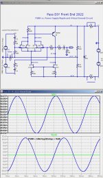
The first image shows the output from the DIY2022 FE when the inputs are shorted, and the power supply has either no ripple (green) or 140mV p-p ripple (blue). The output has about no ripple (green) or 4mV p-p ripple (blue).
The primary reason for this is that the virtual ground circuit is acting as a 50:50 voltage divider between the filtered positive and negative rails, thus VG is modulated by 1/2 the voltage between the filtered rails. The second image shows that the signal on VG is added to the output of the FE.
The third image shows a simple modification to the virtual ground circuit that fixes this issue. The virtual ground DC level is derived from the R11/R12 voltage divider, but the AC component is derived from the external ground, used by the power supplies and the OS stage. The output ripple has been reduced from 4mV p-p to about 21uV p-p.
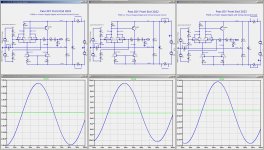
The fourth image is a collage of three configurations: V+/Gnd/V-, Gnd/V-, V+/Gnd, selected by where gnd attached to the power supplies, and which jumper is used across R9, R10, or C5.
The first image shows the output from the DIY2022 FE when the inputs are shorted, and the power supply has either no ripple (green) or 140mV p-p ripple (blue). The output has about no ripple (green) or 4mV p-p ripple (blue).
The primary reason for this is that the virtual ground circuit is acting as a 50:50 voltage divider between the filtered positive and negative rails, thus VG is modulated by 1/2 the voltage between the filtered rails. The second image shows that the signal on VG is added to the output of the FE.
The third image shows a simple modification to the virtual ground circuit that fixes this issue. The virtual ground DC level is derived from the R11/R12 voltage divider, but the AC component is derived from the external ground, used by the power supplies and the OS stage. The output ripple has been reduced from 4mV p-p to about 21uV p-p.
The fourth image is a collage of three configurations: V+/Gnd/V-, Gnd/V-, V+/Gnd, selected by where gnd attached to the power supplies, and which jumper is used across R9, R10, or C5.
Attachments


The logic of using what you already have in your parts bin, especially if it meets or exceeds what is required to get the job done.What logic?
If your parts bin is empty then purchase the parts that fall within your budget that do the job.
We understood very well what was written. It was not useful in my opinion to point out that you had heaps of them while others are looking for them and do not find any. I think it is useless to say more and focus on the subject. And as it was specified the entire point of this circuit is to use J113.
You attacked a member for simply stating reasons for using parts he is having ........
is that rude ...... or is it just rude .....
edit:
as is case with any circuit published by Pa, entire point is to use brain
go figure
is that rude ...... or is it just rude .....
edit:
as is case with any circuit published by Pa, entire point is to use brain
go figure
Last edited:
Both LSK's and 2SK's are available from the Store so not difficult to built using exotic components. It will lower distortion compared to J113 according to NP's measurements.
https://diyaudiostore.com/collections/frontpage/products/matched-jfets?variant=39335247052873
https://diyaudiostore.com/collections/frontpage/products/matched-jfets?variant=39335247052873
There also seem to be some 2SK170BL available here.
https://www.diyaudio.com/community/threads/genuine-toshiba-transistors.395284/
https://www.diyaudio.com/community/threads/genuine-toshiba-transistors.395284/
This is great opportunity to experiment - simple circuit and inexpensive. Good playground for all ideas being presented here and why we should worry about Component change suggestions. And I keep seeing many old Original Toshiba JFET's coming out from different sources. Along with SMD Toshiba parts that can be substituted. I am just waiting for the Store availability as i do not have time to design the PCB. Let us hear from all their observation comparing the original to mods. I would like to see use of this for replacing IC opamps and check the sound- when do we see the Store availability?
kannan
kannan
I've been working on a higher voltage (±32V rail) version of this circuit that could maybe drive a SIT OS, and the following is where I am. Caveats:
1) For dissipation, replaced PNP with a ROHM 2SAR574D3 in an SMD package, which should be hand solderable. It's still a cheap and available part.
2) A buffer stage was added to drive a capacitive load. LTSpice shows lower limit 2kohm II 5000pF. (Will this drive Tokin THF-51S?)
3) Current sources are modified for dissipation and quiescent currents of 3mA, 23mA, and 24mA, in the three legs, L-R. These were tweaked with LTSpice. I think J109s will be better than J111s there, but I'm too lazy to find J109 Spice parameters (so ASC file shows J111).
4) J111s were chosen over J113 because I have a large stash of them, but I've since purchased a few J113 which could be used instead.
5) I don't expect items 3 and 4 above to affect performance much, but I fully acknowledge items 1 and 2 will alter the performance of the original circuit.
I've purchased parts, but have not soldered anything yet. BOM cost is about $38/channel, mostly due to the filter caps which I chose as polypro types (27.5mm pins) at about $2.65 each (qty 10). The MOSFETs cost about the same as the terminal blocks ($1.60 ea.). Of course if I do a PCB layout, the larger caps will drive up the cost due to the extra real estate they'll occupy.
Thoughts?
Attachments

First time I've ever seen a 1.0 ohm resistor used as source degeneration in a constant current source (R17). Dropping, what, sub-60 millivolts? Yowzers.
With the buffer state, the 2nd stage (Q5, M3, Q7) is driving the very light load of the buffer M1 compared to driving the SIT of the OS and can be have a bias current in the 6ma-10ma range, such as in the DIY FE.
That's just a placeholder, sorry. No resistor there produced the reasonable current that looked good for LTSpice, but I figure I'll need some value. Pretend it's whatever value that works (for 24mA, says simulation).First time I've ever seen a 1.0 ohm resistor used as source degeneration in a constant current source (R17). Dropping, what, sub-60 millivolts? Yowzers.
With the buffer state, the 2nd stage (Q5, M3, Q7) is driving the very light load of the buffer M1 compared to driving the SIT of the OS and can be have a bias current in the 6ma-10ma range, such as in the DIY FE.
I thought so too, and that might turn out to be true. But with less than 23mA in that leg and the capacitive load, for some reason I'm getting this kind of stuff (here with 15mA-ish):

I thought so too, and that might turn out to be true. But with less than 23mA in that leg and the capacitive load, for some reason I'm getting this kind of stuff (here with 15mA-ish):
wait, what was that again ZM?I've told ya......... OLG, NFB, CLG
all in all, leave R6 as is
everything else will fall in right place, when you set R7 by output offset
😵
This will improve the thermal stability/drift, in my experience. .5 would have been enough probably too.First time I've ever seen a 1.0 ohm resistor used as source degeneration in a constant current source (R17). Dropping, what, sub-60 millivolts? Yowzers.
Using Parts I have:
Added a follower like in the diyopamp.pdf figure 14
So J111 CCS, K170 LTP , KSA992 & KSC2690 follower with CCS
elana silmicII from ACA for input caps
added trimpot for LTP CSS (not sure if it does any good)
Jumpers for single or dual supply's
jumpers for bal or single inputs
~3ma for ftend
~9ma for A992
~15ma for C2690
seems to work good, tested into 10kR/1nF load


and tested into 50R phones

Thanks
Added a follower like in the diyopamp.pdf figure 14
So J111 CCS, K170 LTP , KSA992 & KSC2690 follower with CCS
elana silmicII from ACA for input caps
added trimpot for LTP CSS (not sure if it does any good)
Jumpers for single or dual supply's
jumpers for bal or single inputs
~3ma for ftend
~9ma for A992
~15ma for C2690
seems to work good, tested into 10kR/1nF load
and tested into 50R phones
Thanks
That's kinda funny that you just posted that. I will be working on my own figure 14-B, just gathering a few parts and final details / ideas before I make the attempt. In fact the .pdf was already open on my browser 😀 I'm going to run my 3rd stage current a bit higher than yours. And my LTP is cascoded (+/- 28 volt rails). But otherwise pretty similar. I'm finishing up my power supply do-over right now. Changing from a cap multiplier to a CLC. 2nd monoblock about half way done. Then I'll start this new front end.
How did you do that? I've spent the past week trying to test J109 and J111s I already had. I haven't found any with Idss less than 90mA, and they're usually >>100mA. When I purchased them, I thought that, with rated values of 40 and 20 min. respectively, they should be more flexible than 2mA parts and easy to adapt to lower currents, but the DS doesn't prepare for how high the actual value can be. I only thought "How much higher could they be?", to paraphrase Homer Simpson.🙂 (A freakin' lot.)Any reason Not to use J111's?
...
these were matched for IDSS only
At these actual levels you're flirting with max. Pd or at least heating the device enough so that it's hard to get a steady state reading. If you lower Vds, you may leave full saturation. Frustrating.
Next I broke down and just bought 10 pcs J113. From the first 5, Idss ranges 26-31mA. That's more like it. I can see why NP (and more experienced DIYers) choose that one. However, I haven't found even two yet that are really close matched.
Having realized this task was getting to seem more like dialysis 😏 , I thought about buying Toshiba SMD or Linear Systems parts; at least they're spec'ed over small Idss ranges for each grade. But then I remembered I still have several JFE2140. Lower noise and already matched. Even economically, they're not much more expensive when you don't have to grade, sort, and discard cheaper parts. If I miraculously get 2 matched pair of J113 from 10 pcs, it's about $3.60 plus much work and less tight matching, rather than ~$9 of TI parts that should be way better.
It may be defeating the whole the cheap legacy novelty point of the design, but this seems to make way better sense to me. I will still use J109s and J111 for CCS parts. Without worrying about matching or Idss, I know how to test (and have used) them for that quite successfully.
If starting from scratch (no parts on hand), I like the idea in the companion thread, using Toshiba SM parts with T/H headers that are very cheap on eBay. There's still some hassle there, though. Maybe I'd just buy J113 in bulk and start over. (Listen to Pa, I guess is the moral here.)
when you have parts with damnbigIdss, and you want to group them, just introduce some source resistance (degeneration)
it'll decrease standing current and you'll be able to group them in safe way, without overheating
it'll decrease standing current and you'll be able to group them in safe way, without overheating
- Home
- Amplifiers
- Pass Labs
- DIY Front End 2022