On the same topic, I must have been blind to use TTA/TTC transistors for Q105-106 having KSA1142/C2682. I used these for Q11 and Q13 in EF3-3 but TTA/TTC for Q105-106 with PS voltages of about +/-72. In my EF3-4 I used KSA1142/C2682 in both cases that is for Q11 & Q13 and Q105-106 although PS in my EF3-4 was lower: +/-64V. Now I'll have to replace TTA/TTC in my EF3-3 with KSA1142/C2682 for Q105-106. Hopefully pcb will allow for that change without any harm done.
In the case of Q101 - 102 TTA/TTC are OK as C-E voltage drop is just above 1V where these two transistors have IC at their MAX of over 1A. No heatsink needed.
In the case of Q101 - 102 TTA/TTC are OK as C-E voltage drop is just above 1V where these two transistors have IC at their MAX of over 1A. No heatsink needed.

TTA/TTC have higher gain than the 3503/1381 - typically ~220 vs ~80-130 , so are preferred at Q101/102 as this is the capacitance multiplier. Higher gain = better rail smoothing, and rail voltage isn't so much of a concern in this part of the circuit compared with the predriver position.
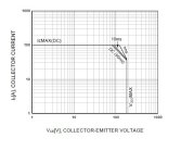
The Predrivers Q105/106 are running class A. Here is the temperature derated SOA for KSC3503 vs TTC004B, well within the DC SOA using a heatsink.

Exactly. Actually a few other transistors could be used here such as ksa1220y/c2690y, 2sa1249t-s/c3117t-s, 2sa1930/c5171, 2sa1209t/c2911t as these have even higher Hfe than 3503D/1381E as F are no longer available. KSA1142y/C2682y could be used as well but are too precious for other applications such as predrivers Q105-106.
Supposedly Profusion will have KTC3503/KTA1381 in stock in January of 2025
https://us.profusion.uk/int/audio/transist/driver-transistors
https://us.profusion.uk/int/audio/transist/driver-transistors
Thanks GianLuca, I love to deduct costs in these trying times. I might order it soon.They are pretty much the same chassis, the main difference is the width which goes from 373 to 255. The prices you see are VAT included but assuming you order from Australia you have to deduct 22% 🙂 Here is a picture of the MiniDissipante 4U to give you an idea of how it can look like https://modushop.biz/site/index.php?route=product/product&product_id=877
I confirm this chassis can have the heatsinks drilled according to the Wolverine specs
SOA of KSA1142/C2682. Vceo 180V, Cob 4.5pF, Ft 180MHz. Unfortunately now obsolete. Luckily still have a few. Managed to desolder TTA/TTC from EF3-3 pcbs (Q105-106). Not easy to do that on two-sided pcbs. Luckily did not damage them. Then replaced TTA/TTC with KSA1142/C2682 but made a mistake swapping their locations because on the schematic I wrote KSA1142 next to TTC and KSC2682 next to TTA as better options. Must be getting too old for building amps.
Attachments
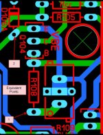
On the pcb two R109 connections (pins) are connected/shortened. Set your pot in such a way that its two corresponding pins are also shortened (zero resistance) so 500 ohm is between the two shortened tracks and the third one.
Please read point 22.2.C of the build guide and refer to the markings on you pcb silkscreen to know which is pin 1 and 2 so you can measure the resistance in the correct location.Getting ready to test my 2nd channel and want to make sure I set R109 correctly.
Have I mapped this out correctly?
If you board is installed you can check here.
Just verify the resistance and the direction you need to turn the pot with your DMM prior to turn on.
Attachments
Hello. Sorry but I can't find the values of Cx, Cs and Rs (Quasimodo circuit), the secondaries of the transformer are 45.5 V
Thank you
Thank you
You need to read the Quasimodo documentation and build the test rig. The values for Cx and Cs are in the Quasimodo documentation and the value of Rs is calculated by the test rig.Hello. Sorry but I can't find the values of Cx, Cs and Rs (Quasimodo circuit), the secondaries of the transformer are 45.5 V
Thank you
I'm thinking I'm dyslectic regarding this pot install. Just don't want to light up my new board. Already done that once. So, is this clear, and correct?Please read point 22.2.C of the build guide and refer to the markings on you pcb silkscreen to know which is pin 1 and 2 so you can measure the resistance in the correct location.
If you board is installed you can check here.
Just verify the resistance and the direction you need to turn the pot with your DMM prior to turn on.
My new left board will be installed with the output transistors down vs. the right board's transistors will be on top. For the right board the R109 was installed with 123 on the pot aligned with 123 markings on board. I measured resistance with with + DMM lead on 1 and - lead on 2 which showed 450R. To bias in this position I turned the pot left.
For the left pot I inverted the pot so that 1,2,3 were reversed vs the board markings. I measured the pot with red DMM lead on 3 and - on 2. I measured 450R resistance. To bias this pot I will turn the dial right.
OK, slow down. On the left board you said you measured on the 3 and 2 pins. Is that the the 3 and 2 stamped on the board? If it is, then you are wrong. The circuit didn't change on the board because you flipped the pot. You still measure between 1 and 2, but it will adjust the opposite direction.For the left pot I inverted the pot so that 1,2,3 were reversed vs the board markings. I measured the pot with red DMM lead on 3 and - on 2. I measured 450R resistance.
Rick,
Thanks, you articulated what I couldn't. The circuit doesn't change. Just the orientation of biasing direction.
Got it.
Thanks, you articulated what I couldn't. The circuit doesn't change. Just the orientation of biasing direction.
Got it.
Two questions:
1. C118 & C119 = 470pF. Are these optimum values for Sanken drivers 2sa1859a/c4883a or just universal because of mje1503x?
2. I have EF3-4 v3.9 board and populated it using v4.2 BOM version, which shows notably different resistor values in the bias circuit than v4.3. Eg R105=1.4k in V4.2 and 1.8k in v4.3, R106=3.9k in v4.2 vs 1.2k in v4.3, R108=560 in v4.2 vs 430ohm in v4.3. Transistors I used for Q103 and 104 are BD139-16.
Of these resistor R106 values are substantially different between v4.2 and v4.3. Is it because in v4.3 Q103-104 transistors are mje340, while in v4.2 are BD139-16 so resistor values have been optimized for transistors used in each of these versions?
y tho? you sure you reading the rows right? there are different values for those resistors depending on how you choose to mount your driver transistorsI have EF3-4 v3.9 board and populated it using v4.2 BOM version
I'm still lost - I see no difference between 1st GB, 2nd GB, and 4th GB BOMs for R105-108. (may 2024 versions). Are you perhaps looking at outdated BOMs from 2022 that incorporated the older original bias management circuit? The only BOMs you should be referencing are the May 2024 versions, if you are populating new boards. You can use older BOMs if you insist, but do not mix and match, could lead to smoke.
I also cannot find a BOM version 4.3. (only 3.9 - 1st GB, 4.2 - 2nd GB & 4.4 - 4th GB), however I assume you mean 2nd GB BOM, as the schematic is titled V4.3.
The reason I said "y tho" - If you have 1st GB boards, that is IPS board v3.7 and EF3-X v3.9, I strongly advise you only use the 1st GB BOM - latest dated 22 May 2024. For example, D101-102 is missing from 2nd GB BOM which could cause a builder confusion.
***
While we are on the subject of the 1st GB BOM - there is one minor error still present in it if you are using MJE drivers; the part C5 lists a CD19 part when it should be a CD15 part - the leg spacing is a bit wide on the CD19. You can make it work though 🙂
I bought these boards well over a year ago, I think in 2023 and started populating these a year ago using BOM May 2023 (v4.2). It's done and was done before May 2024. But looking at circuit diagram for version 4.3 I have noticed a number of differences in component values, especially in the BIAS circuit. And one of these differences was R106=3.9k in BOM May 2023 and R106=1.2k on the diagram for v4.3. That's a substantial difference. I wondered why such a difference? Is it because in BOM 4.2 BIAS recommended transistors are BD139-16 while on the v4.3 diagram as well as in the BOM1 MJE340 transistors are used? Or these resistor values are PS voltage dependent but somehow in BOM May 2023 (v4.2) it is not stated? BOM May 2023 (v4.2) does not differentiate BIAS resistor values for different PS voltage values.
Resistor values in BOM March 2023 (v3.9 board) in the BIAS circuit are the same as on the v4.3 schematic for +/-64V rails. My EF3-4 will use +/-64V PS so what resistor values (R105-108) should be used in this circuit? In BOM May 2023 resistors R105-R108 are different only for EF3-3 and EF3-4 boards and are PS voltage independent, while resistors such as R6, R15, R17, R23, R24, Rled are shown as PS voltage dependent.
Following the above what BIAS circuit resistor values (R105-108) should be used with EF3-3 and PS +/-71 voltages? as my EF3-3 boards will see +/-71V PS.
- Home
- Amplifiers
- Solid State
- DIY Class A/B Amp The "Wolverine" build thread