Not specifically, I tested my boards on my bench with an isolation mat underneath, to ensure no shorts from any stray metal on my bench..
What you need to pay attention to - Section 22 in build guide v41
--- V+ on IPS goes to +30Vdc on your bench power supply
--- V- on IPS goes to -30Vdc on your bench power supply
--- G1 on IPS goes to GND on your bench supply
--- Connect PD+/ND-/NFB all 3 connections to Ground (I used alligator clip wires, above pic shows using a bread board with jumper wires, either is fine)
- Section 22, specifically says to also connect C1 to G2
Then with current limited (I think 0.5a is enough for one IPS board), power it up and follow the Section 22 step-by-step to verify functionality and set CCS and check DC offset, etc.
Before powering anything - triple check your wiring with a DMM that all connections go to the right location. diode check to make sure PD+ / ND- / GND / NFB and C1 go to G2. You can confirm C1 goes to G2 with your DMM, I don't specifically remember using a wire to connect these, but did check to make sure there was connection to G2 at all these points.
Pic below is terrible - but hopefully you get the idea. I'm a visual person.
Normall you wouldn't ground the output. That way you could measure DC offset on the output.Not specifically, I tested my boards on my bench with an isolation mat underneath, to ensure no shorts from any stray metal on my bench..
What you need to pay attention to - Section 22 in build guide v41
--- V+ on IPS goes to +30Vdc on your bench power supply
--- V- on IPS goes to -30Vdc on your bench power supply
--- G1 on IPS goes to GND on your bench supply
--- Connect PD+/ND-/NFB all 3 connections to Ground (I used alligator clip wires, above pic shows using a bread board with jumper wires, either is fine)
- Section 22, specifically says to also connect C1 to G2
Then with current limited (I think 0.5a is enough for one IPS board), power it up and follow the Section 22 step-by-step to verify functionality and set CCS and check DC offset, etc.
Before powering anything - triple check your wiring with a DMM that all connections go to the right location. diode check to make sure PD+ / ND- / GND / NFB and C1 go to G2. You can confirm C1 goes to G2 with your DMM, I don't specifically remember using a wire to connect these, but did check to make sure there was connection to G2 at all these points.
Pic below is terrible - but hopefully you get the idea. I'm a visual person.
View attachment 1372844
@Moderator - please delete Post #4,781 - invalid pictorial
@jwilhelm you are absolutely correct - read my own build picture wrong. PD+/ ND- / NFB all go together, with V+ and V- getting +/-30Vdc
THEN make sure you have GND connected, I clipped G1 and G2 together to my bench power supply.
Daniels picture is really good - copy to a separate tab and blow up on your computer and you can easily follow the leads
Lathes - who needs lathes 😉?
The way I did it was crude, but it worked pretty well. I call this the "handheld wobbly lathe". Using an old speaker crossover inductor as my wire, I slid one end of the wire into the chuck of a cordless drill alongside a 12mm (new, not rusty) drill bit and clamped the chuck down so one of the chuck teeth clamped the wire. You need the drill bit sitting quite a way out of the chuck, so you get "clean" former and don't run up into the cutting spirals. The drill bit sits crooked, but this is no concern. I wound out some wire and held the remainder in other hand and began to slowly, whilst holding the inductor tight to keep the wire under tension, wind the new coil onto the drill bit. You can place the cordless drill in a vice or press it down flat on a bench if you need the extra strength. I wound well past the amount of turns I needed, then keeping the tension on, vice clamped the excess to the end of the drill bit. Cut away the remaining old inductor and apply glue over top of the whole formed coil but don't get glue on the drill bit or you won't get the coil off. When dry, unclamp and unwind the coils you don't need. Slip the coil off the drill bit - back the short way not over the cutting spirals. You will likely fail the first couple attempts, but I got better each time until I got nice, neat tight coils. Now I have done about 6 ultra neat coils. If you use an old drill bit you also wont get the coil off the drill bit.
Its stupid, but it work.
I like this. I was trying to figure out a way to clamp the wire and wind it. I'll try it.
Thanks,
John
Everything you need is in the attachment in my post above #4782. I can't take anymore, I'm done.
Carefully follow each wire on the Right, to where it aligns with the IPS board. Green = GND, BLUE = V- and RED = V+. Then NFB, PD+ and ND- are all linked together with jumper wires.Which is Daniels picture?
If you are repairing a board that has had thermal issues or blown outputs/drivers - Another step you can take to ensure no current hogging (some getting really hot and some cool) of outputs is before you liven up check resistance from OUTPUT to each output transistor emitter leg, make sure no shorted or blown open emitter resistors. Should be 0.21 to 0.25 ohm depending on your chosen emitter resistors. If you reassemble everything and have missed a blown/dead emitter resistor, you are going to cause some outputs to current hog and probably blow again.
Agree with others - test your IPS separately and rule out any issues there, that's half the job done.
Agree with others - test your IPS separately and rule out any issues there, that's half the job done.

I have a question about R17. The guide says to use a 9.1K resistor in parallel with the one installed on the input board. I have installed a 12K 1W per requirement to match my Cobra's +/-63.64V output. If parallel means equal in this case, shouldn't I use a 12K on the back side of the board?
Attachments
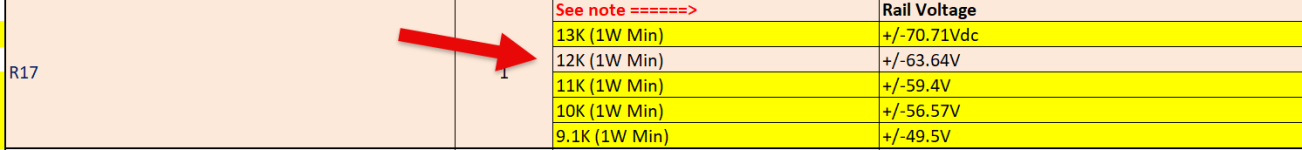
Read the sentence. The term parallel refers to how the part is connected, it is a VERY basic electrical term. Look up the terms parallel and series connections, you should know this.The guide says to use a 9.1K resistor in parallel with the one installed on the input board.
Feel free to PM if you need a hand with this Chiptech, I think there are some pictures of the build in the video series which could help here also early on in this thread or the build guide.I have a question about R17. The guide says to use a 9.1K resistor in parallel with the one installed on the input board. I have installed a 12K 1W per requirement to match my Cobra's +/-63.64V output. If parallel means equal in this case, shouldn't I use a 12K on the back side of the board?
Rick,Read the sentence. The term parallel refers to how the part is connected, it is a VERY basic electrical term. Look up the terms parallel and series connections, you should know this.
You are right. I can do better. I'm going to take a mulligan for that question. I swam this afternoon, which always knocks me out and I should have taken the afternoon off.
Good progress this weekend, getting ready to bench test.

Almost all the transistors failed. One cause I suspect is that I didn't have effective grease cover. I'd appreciate any views on this from the photo.
Of course, the other reason was the failure to remove R17 and J103. Ouch. Won't make that mistake again.
Of course, the other reason was the failure to remove R17 and J103. Ouch. Won't make that mistake again.
Attachments
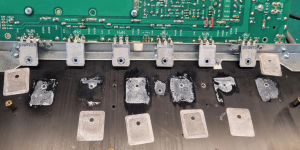
Check the transistor mounting holes are deburred and flat with no swarf please.Almost all the transistors failed. One cause I suspect is that I didn't have effective grease cover. I'd appreciate any views on this from the photo.
Of course, the other reason was the failure to remove R17 and J103. Ouch. Won't make that mistake again.
Attachments
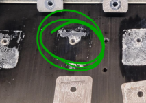
This can also be caused if your screw holding the transistor down is bottoming out in the hole before actually clamping the transistor the heatsink
That's a very good point.This can also be caused if your screw holding the transistor down is bottoming out in the hole before actually clamping the transistor the heatsink
- Home
- Amplifiers
- Solid State
- DIY Class A/B Amp The "Wolverine" build thread