Thanks for the link.
I tried your suggestion today, and the faint noise in the left tweeter is now gone! 🙂
Still need to tighten and zip-tie the remaining cables, but this is the new layout.

Personally I wouldn't run a input wire parallel with the output transistors.Thanks for the link.
I tried your suggestion today, and the faint noise in the left tweeter is now gone! 🙂
I personally think that you would be better to running it as I have shown it the image below.
Use one of you bridge to get the input wire away from the DC power leads. Run the input wire high on the front panel and around the top of your amplifier board. This is the lowest noise side of the amplifier board.
Attachments
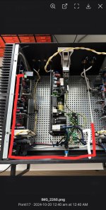
One may also run under the grid. I have done that on many builds with very good results. The grid tends to act like a Faraday... just say'n that also negates the longer wire.
Can I ask why you positioned the Cobra vertically? ThanksThanks for the link.
I tried your suggestion today, and the faint noise in the left tweeter is now gone! 🙂
Still need to tighten and zip-tie the remaining cables, but this is the new layout.
View attachment 1369715
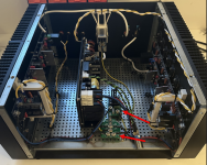
can I inquire as to the function of these two boards, see below. ThanksWired my Wolverine today and gave it the first listen. And wow, not sure if it's because of all the work that have gone into it, but it sounds really good on my not so fancy speakers. The sound feels very controlled and yet with lots of power (and now i will use no more meaningless audiophile jargon 🙂 ).
It was difficult to finalize on a good wiring scheme, especially since i have no skills whatsoever in working with metal (nor any tools), making it difficult to create new mounting points for wires. I do however have a 3D printer, so i printed some plastic wire "bridges" in ASA plastic. The result might be kind of stupid, but it works pretty well.
My fairly sensitive speakers are nearly dead quiet when the amp is on, except for the faintest buzz when i have my ear pretty much touching the tweeter of the left speaker. I have a feeling it might be due to the sub-optimal placement of the left input wire right next to the output of the right channel. I will have to optimize the wiring a bit before finally putting the top lid on it, but it's difficult to stop the music and unplug it from the wall.
All in all, for those currently building one, you should be very excited to hear it when it's done 🙂
View attachment 1369431
View attachment 1369432
Attachments
I have been using fast blow fuses. But I just noticed that the fuses specified in the BOM are all slow blow. Which should I use under full power [64DCV]?Use 6 or 8 amp rail fuses. 6 for most cases, 8 if you often listen loud or parties, 10 if you are driving horribly inefficient speakers (lower than 84dB) at party levels.
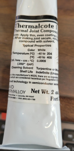
I used the Thermalcote, which I had on hand. Not sure how old it is either.What's the part number of the thermal compund you used? Many compunds are electrically conductive and will eventually work their way to somewhere they shouldn't and blow the fuses.
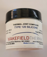
I propose to use the Wakefield silicone type 120 as shown below. Can't find the product number for it. Please advise if there is a better product I should use. I only want to remove, test the outputs and replace once.
Attachments
Thanks for the suggestion Stuart! I can see why this would be an even more optimized wiring scheme. Will have to dwell a bit on the best way to do it. I lack easy mounting points on the front panel, as well as on the other side of the amplifier board. Though i guess nothing is impossible when you're armed with zip ties and a 3D printer 😀Personally I wouldn't run a input wire parallel with the output transistors.
I personally think that you would be better to running it as I have shown it the image below.
Use one of you bridge to get the input wire away from the DC power leads. Run the input wire high on the front panel and around the top of your amplifier board. This is the lowest noise side of the amplifier board.
It was really only based on convenience. It was easy to mount the Cobra this way, and left lots of space to either amplifier board. In the future i might be interested in implementing speaker protection, and wanted room on the base plate to mount boards.Can I ask why you positioned the Cobra vertically? Thanks
The board with the heatsink is a GND lift. It "separates" amplifier ground and chassis ground. It's my first time using something like this in a build, but i have previously been victim of nasty, hard-to-understand ground issues in my systems so i wanted to try and use one here.can I inquire as to the function of these two boards, see below. Thanks
The other board is kind of like a star ground, but as a "T" instead. Where high and low current return paths are placed in optimal order.
BTW these boards are not my designs, they are mentioned several times earlier in this thread. If i remember correct they are stuartmp's design, and they should be available on pcbway i think. 🙂
I would just print off some cable holders which you can apply some good quality 3M double sided tape to.I lack easy mounting points on the front panel, as well as on the other side of the amplifier board. Though i guess nothing is impossible when you're armed with zip ties and a 3D printer 😀
Or purchase something like this.
Cable holder
It may also be a good idea to run the DC power wires that run to the amplifier board under the mesh base plate as @thompsontechs suggested
Last edited:
I can't see the part number on the Thermalcote. I think 249 is non-conductive (electrically) but 250 is. The Wakefield 120 is definitly okay.I used the Thermalcote, which I had on hand. Not sure how old it is either.
I propose to use the Wakefield silicone type 120 as shown below. Can't find the product number for it. Please advise if there is a better product I should use. I only want to remove, test the outputs and replace once.
Great thanks. I also just noticed that I used two mica insulators with the Q103. That didn't help things.
When I replace the output transistors I will use a much smaller amount of silicone on both sides of the Mica insulators.
When I replace the output transistors I will use a much smaller amount of silicone on both sides of the Mica insulators.
Having removed the six output transistors, the results are in. I fried one PNP and the adjacent NPN.
To recap, I used incorrect thermal grease, used too much of it, and I had two mica insulators on Q103 and one of the output transistors.
On the first day of one-hour elapsed time, I was struggling to hold at ~40mV. I shut down and resumed on day two. I appeared to be getting more stability for about 45-50 minutes and then the bias fell and a short occurred.
I will rebuild the board and start over with initial testing using my DC power supply.
Any other learning I should take away from this?
And thanks for all the help.
Upon further reflection I will start with 15.1 initial testing. to make sure nothing is amiss. Does that require that I remove and test all the transistors on the input board?
I can't imagine how this,two mica insulators or a little more greace was the reason for faults.🤔Great thanks. I also just noticed that I used two mica insulators with the Q103. That didn't help things.
When I replace the output transistors I will use a much smaller amount of silicone on both sides of the Mica insulators.
The only possibility.. if greace is conductive.
You asked a good question:
Answer: Thermalcote Thermal Joint I Compound is a silicone-based thermal grease designed to improve the transfer of thermal energy across metal-to-metal interfaces, such as between a transistor or rectifier case and a heat sink1. It is not electrically conductive but has excellent thermal conductivity, which is more than 15 times that of air and more than 4 times the conductivity of typical silicone-based greases.
Now I don't have a good theory of what caused the short.
What I know is that Q111 Q114 and the resistors R124A and R124B for each transistor are fried. All the rest of the parts I can use probes on for both boards appear ok.
Short of removing all the parts, does it make sense to replace the damaged parts and retrace all testing steps starting at 17. initial power up?
Read the label. On the bottom right there is a part number of what version you have. The part number was cut off in your picture.
- Home
- Amplifiers
- Solid State
- DIY Class A/B Amp The "Wolverine" build thread