Are you able to post some clear high resolution photosRickRay:
Yes, the pot next to TP1 and TP2 is R11, and the best I could get from adjusting it was 611 mV (L ch) and 133 mV (R ch). And yes, I'm using the TTA and TTC FETs. The readings across R111A and R111B started out lower (about 780-790 mV) and slowly rose, settling at 810 mV (L ch) and 819 mV (R ch).
Regards.


Thanks for this.Hi everyone,
As promised, here is the next video in the Wolverine YouTube Build series I am doing.
I hope you enjoy watching it:
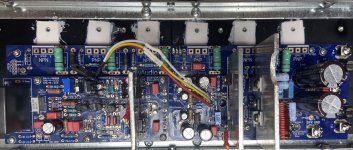
Also, for the people building the Wolverine amplifier please see the feedback trace I used in the photo below.
- Dan
I notice the use of coherent averaging function when taking distortion measurements with the magnifier. Now, its likely my understanding is wrong, but I though the use of coherent averaging could only be used to capture THD, and was not valid for true THD+N and noise measurements i.e. making the THD+N number moot.
I hope I'm wrong, because that amp is putting up some serious numbers!
Thanks for the nice comments Mainframe99,Thanks for this.
I notice the use of coherent averaging function when taking distortion measurements with the magnifier. Now, its likely my understanding is wrong, but I though the use of coherent averaging could only be used to capture THD, and was not valid for true THD+N and noise measurements i.e. making the THD+N number moot.
I hope I'm wrong, because that amp is putting up some serious numbers!
I will have a look into this, regular averaging have a cleaner looking FFT if I remember correctly.
I actually saw better numbers at one point...
- Dan
Please check your Dale RN60 1K resistors, they look 100r to me...
-Jan
-Jan
Jan:
Holy $#!^. What a maroon! Great eye - thank you!
This is such a fabulous community.
Regards,
Scott
Holy $#!^. What a maroon! Great eye - thank you!
This is such a fabulous community.
Regards,
Scott
As I have checked everything I discovered that I had the two capacitors in my snubbers switched. I am continuing to rearrange parts to reduce loop areas and proximities, but more than likely the switched caps are why I have so much 60Hz and odd harmonics.
Folks:
Okay, things have progressed but I'm not out of the woods yet. I have been following the Build Guide on a step-by-step basis and am now at Sections 18.H and I. I'm testing just the left channel. J103 has been removed, all 6 LEDs light, the output drivers are properly installed and CCS has been adjusted to precisely 5.0 V. What seems odd is that the reading across R111A and R111B is a steady 0.843 V and the DC offset across TP101 and TP102 is rock solid at 0.00 mV. In fact, minor adjusting of R25 has no effect on DC offset -- it doesn't change from 0.00 mV and the minimum reading across R111A and R111B is 0.843 V -- I can't reduce it to 40 mV per Build Guide 18.I.
Suggestions appreciated!
Regards,
Scott
Hi Scott its late here so if R109 is set to maximum resistance and you have 0.843V measured between TP101 and TP102 Shut it down and investigate further as that means your pulling 1.9Amps though each collector of the output transistors... not good.Folks:
Okay, things have progressed but I'm not out of the woods yet. I have been following the Build Guide on a step-by-step basis and am now at Sections 18.H and I. I'm testing just the left channel. J103 has been removed, all 6 LEDs light, the output drivers are properly installed and CCS has been adjusted to precisely 5.0 V. What seems odd is that the reading across R111A and R111B is a steady 0.843 V and the DC offset across TP101 and TP102 is rock solid at 0.00 mV. In fact, minor adjusting of R25 has no effect on DC offset -- it doesn't change from 0.00 mV and the minimum reading across R111A and R111B is 0.843 V -- I can't reduce it to 40 mV per Build Guide 18.I.
Suggestions appreciated!
Regards,
Scott
Reading you messages again. I think your measuring the wrong thing. R111A and R111B should be about 1.3v so you will need to reduce the resistance on R109.
R109 adjusts the bias measured at TP101 and TP102. You say DC offset in your message above
DC offset is measured TP104 to TP100
We only need to measure R111A and R111B when the output transistors are not installed.
Last edited:
stuartmp & Co.:
Hmm, using the wrong terminology is only part of my problem. Okay, I've restarted my effort with the left channel.
CCS (R11) is very close to 5V (ranging between 4.95 and 5.02V).
The reading across R111A and R111B starts out at 1.49V when the channel is cold. Over the next 5-10 minutes, the reading slowly drops to about 1.21V.
DC offset (TP104 and TP100) is reading in the 1.9mV to 2.2mV range.
And yes, the 3U heatsink is pretty toasty.
Does this sound OK? If so, I'll move to the right channel. I don't want to screw up the second channel until the first channel is testing reasonably well.
Many thanks,
Scott
.83V across R111A and R111B would explain why you don't get any reading other than 0mV across TP101 and TP102 because there isn't enough voltage to turn on the output stage. There should be ~1.2V across R111A and R111B (driver bias resistors) and 40mV across TP101 and TP102 (output emitter resistors) for ~90mA bias per output pair. Adjust R109 to bring up the bias. Are you confusing DC Offset with the bias adjustment?Folks:
Okay, things have progressed but I'm not out of the woods yet. I have been following the Build Guide on a step-by-step basis and am now at Sections 18.H and I. I'm testing just the left channel. J103 has been removed, all 6 LEDs light, the output drivers are properly installed and CCS has been adjusted to precisely 5.0 V. What seems odd is that the reading across R111A and R111B is a steady 0.843 V and the DC offset across TP101 and TP102 is rock solid at 0.00 mV. In fact, minor adjusting of R25 has no effect on DC offset -- it doesn't change from 0.00 mV and the minimum reading across R111A and R111B is 0.843 V -- I can't reduce it to 40 mV per Build Guide 18.I.
Suggestions appreciated!
Regards,
Scott
Adjust R109 for Output bias
1) Across R111A and R111B should read ~1.2V
2) Across TP101 and TP102 should read 40mV
Adjust R25 for DC Offset
1) Across TP104 (output) and TP100 (ground)
Jeremy
Last edited:
Correction: The procedure says 40mV in one spot but it should 44mV (100mA per pair)
Adjust R109 for Output bias
1) Across R111A and R111B should read ~1.2V
2) Across TP101 and TP102 should read 44mV
Adjust R25 for DC Offset
1) Across TP104 (output) and TP100 (ground)
Jeremy
Adjust R109 for Output bias
1) Across R111A and R111B should read ~1.2V
2) Across TP101 and TP102 should read 44mV
Adjust R25 for DC Offset
1) Across TP104 (output) and TP100 (ground)
Jeremy
Hi Guy's
I have just updated the Build Guide to make Points 18.H and 18.I clearer.
The current version is now "Wolverine Precision EF3 Build Guide revision 22 (28-08-22)"
Check your Dropbox project folder for the updated file.
Enjoy 🙂
I have just updated the Build Guide to make Points 18.H and 18.I clearer.
The current version is now "Wolverine Precision EF3 Build Guide revision 22 (28-08-22)"
Check your Dropbox project folder for the updated file.
Enjoy 🙂
Jeremy:
Thank you for the clear guidance, and I'm sorry to be such a pain. The left channel now seems to be behaving; across TP101 and TP102 the reading is 40 mV +/- 2 mV (which I will bump up to around 44 mV), and DC offset is now down to below 0.5 mV. It's time to move on to the right channel (which I hope is drama-free).
Much appreciated!
Regards,
Scott
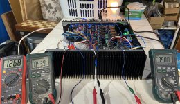
Jeremy, stuartmp & Co.:
In an overabundance of caution, I'd appreciate your feedback on my testing of the right channel.
The left-most DMM is reading across R111A and R111B,
the center DMM is reading across TP101 and TP102, and
the right-most DMM is reading across TP1 and TP2.
I only have 3 meters. In case it's relevant, DC offset is currently in the 0.1 to 0.3 mV range.
In the background (yes, in my laundry room), the 60 watt light bulb in my dim bulb tester remains lit. The fact that it isn't dimming is the reason for my concern.
Do I have reason to be concerned (go ahead, take your best shot)?
Thank you,
Scott
Attachments
I will let one of the other more knowledgeable guys give you the correct answer. But I'm pretty sure you are drawing at least 600mA with the bias adjusted correctly and more like 1.2 amps with both channels running.
1) Turn the bias down (R109) to 10mV across TP101 and TP102 on both channels.Jeremy, stuartmp & Co.:
In an overabundance of caution, I'd appreciate your feedback on my testing of the right channel.
The left-most DMM is reading across R111A and R111B,
the center DMM is reading across TP101 and TP102, and
the right-most DMM is reading across TP1 and TP2.
I only have 3 meters. In case it's relevant, DC offset is currently in the 0.1 to 0.3 mV range.
In the background (yes, in my laundry room), the 60 watt light bulb in my dim bulb tester remains lit. The fact that it isn't dimming is the reason for my concern.
Do I have reason to be concerned (go ahead, take your best shot)?
Thank you,
Scott
2) See if the bulb goes out
3) If the bulb is not lit any more then power down and remove the light bulb current limiter
4) Power up again
5) Set bias using R109 with 44mV across TP101 and TP102 on both Left and Right amp/channels
If the light doesn't go out on Step 2) then something is wrong
Jeremy
Scott, if you have completed and passed all the steps listed in the build guide and you definitely checked all the points listed at 17.B and they were ok then things are looking good.Jeremy, stuartmp & Co.:
In an overabundance of caution, I'd appreciate your feedback on my testing of the right channel.
The left-most DMM is reading across R111A and R111B,
the center DMM is reading across TP101 and TP102, and
the right-most DMM is reading across TP1 and TP2.
I only have 3 meters. In case it's relevant, DC offset is currently in the 0.1 to 0.3 mV range.
In the background (yes, in my laundry room), the 60 watt light bulb in my dim bulb tester remains lit. The fact that it isn't dimming is the reason for my concern.
Do I have reason to be concerned (go ahead, take your best shot)?
Thank you,
Scott
I assume that you are now at step 18.I ?
What is your rail voltage?
Assuming its 57v and your drawing ~650mA then you are drawing ~37W per channel. So the bulb maybe somewhat lit.
Assuming you are only testing one channel and the left channel is not connected. The easiest thing to do is start turning R109 to its maximum resistance settings as you do the bulb should go out.
If it doesn't then there's something you've missed. If it goes out reset R109 and while measuring across TP101 and TP102 to 40mV. Yes 40mV it's intentionally a little lower than the ideal 44 mV due to the current restrictions of the light bulb.
I will need to update the build guide again as I forgot about this point yesterday when I changed it from 40mV to 44mV.
Once current limiting is removed 18.J it its then set to its final value in the burn in procedure.
- Home
- Amplifiers
- Solid State
- DIY Class A/B Amp The "Wolverine" build thread