but at my current speedI am afraid that Nelson is going to beat me to it when it comes to presenting value recommendations
Not very likely.
Looking good! Are those RCAs from WBT?
Greets
Dirk
Thank you, yes they are WBT.
I finally received the four Biamp 6-24 boards, shipping was quick, but not me ordering. I want to use them for a 3-way speaker with active sub in addition. Sub has its own crossover, so I will just give it a full signal. I need two bandpasses, 4th order @ 80-450Hz and 450-2000Hz. Then a highpass 4th order @ 2000 Hz and up to 20kHz.
How can I make it into a bandpass?
How can I make it into a bandpass?
Last edited:
So at this point you know what you want the crossover to do but how to set up with the hardware?
Ideally you want to treat each stereo bi amp pcb as a functional block so you have two stereo bandpass pcb and a stereo high pass pcb. You don't need the low pass for the sub as you have your active crossover.
I have had look at my pcbs which I have not stuffed yet. This is really something Nelson should describe as its his pcb design.
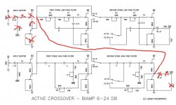
However, the input signal is common to both the Low and High input level trim pots. What this means is that to configure the pcb as a stereo bandpass filter you need to loop the high pass filter output back to the input of the low pass filter.
But the inputs needs to be isolated.
To configure the pcb the signal enters the input designation on the PCB IN. The output of the high pass filter designated HIGH on the pc is looped back with a length of hookup wire to the track that links the -ve input of the 10uF coupling cap next to the LOW level input trim pot. Do not install the LOW level trim pot.
This will cascade the low pass filter from the output of the high pass filter. The output of the low pass signal is taken from the pcb designation Low to your power amp.
The same applies to the other bandpass filter. No alterations are required for the high pass filter.
Set the crossover RC components for the frequencies you require.
The inputs of all three crossover pcbs should be joined to the common signal input from the source.
I think this is correct.
Ideally you want to treat each stereo bi amp pcb as a functional block so you have two stereo bandpass pcb and a stereo high pass pcb. You don't need the low pass for the sub as you have your active crossover.
I have had look at my pcbs which I have not stuffed yet. This is really something Nelson should describe as its his pcb design.
However, the input signal is common to both the Low and High input level trim pots. What this means is that to configure the pcb as a stereo bandpass filter you need to loop the high pass filter output back to the input of the low pass filter.
But the inputs needs to be isolated.
To configure the pcb the signal enters the input designation on the PCB IN. The output of the high pass filter designated HIGH on the pc is looped back with a length of hookup wire to the track that links the -ve input of the 10uF coupling cap next to the LOW level input trim pot. Do not install the LOW level trim pot.
This will cascade the low pass filter from the output of the high pass filter. The output of the low pass signal is taken from the pcb designation Low to your power amp.
The same applies to the other bandpass filter. No alterations are required for the high pass filter.
Set the crossover RC components for the frequencies you require.
The inputs of all three crossover pcbs should be joined to the common signal input from the source.
I think this is correct.
I also have a tri-amping question. I'd like to eq lower frequencies to behave in my room. Can I split off the highs with the 6-24 and feed into an ACN for the bandpass/lows?
Would it be better to use two ACNs for this?
Would it be better to use two ACNs for this?
I'm going to start collecting the bits and pieces for this.
Some quick questions:
Is there any real advantage to the 24db xover when crossing a fullrange to a subwoofer? Feel like fewer stages might be nicer ...
Some quick questions:
- This will be driven by a TVC preamp, so can I omit the input caps, and replace the input pot with 50K resistor?
- The two amps it will be driving have an input impedence of 50K, and 10K respectively - can I lower the size of that output capacitor?
- Is this a unity gain device?
Is there any real advantage to the 24db xover when crossing a fullrange to a subwoofer? Feel like fewer stages might be nicer ...
1. This will be driven by a TVC preamp, so can I omit the input caps, and replace the input pot with 50K resistor?
If you have a look at the schematic in the article of post 1 you will see that removing the trim pots will make the low /high levels non adjustable.
There is dc potential on the other side of the cap do it can’t be removed.
2. The two amps it will be driving have an input impedence of 50K, and 10K respectively - can I lower the size of that output capacitor?
No. Reducing the cap value will introduce phase shift at low frequencies and distortion at low frequencies due to the ac voltage across the cap. I recommend 220uf if it’s a electro cap. Ref Doug Self on capacitor distortion.
Yes3. Is this a unity gain device?
Last edited by a moderator:
Correct
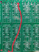
Thanks, you saved my project. Is there no need for a plus and a minus wire when cascading high pass and low pass channels?
You wrote that RCA input should be isolated. Do you mean to just remember to use the plastic spacers to isolate the input connectors from the chassis?
Thanks, you saved my project. Is there no need for a plus and a minus wire when cascading high pass and low pass channels?
Not quite. My post referenced the electrical de-linking of the low pass filter input from the pcb source input track to the low pass trim pot.
The source inputs are in the far left and centre of your image designated IN & G for the left and right channels. As the signal is connected to ground no additional ground wire is required.
You wrote that RCA input should be isolated. Do you mean to just remember to use the plastic spacers to isolate the input connectors from the chassis?
My comments are referring to the isolation of the +ve input signal from the low pass trim pot. This is implemented by not installing the trim pot on the low pass filter. You can use isolated spacers if you wish. The low pass filter is cascaded from the high pass filter so you don’t want the input signal going to the low pass filter.
Your marked up pcb image is correct. You only need the one hook
up wire. For optimal noise the signal ground may need to be connected to your chassis ground.
Call Out.
If there is a revision of the pcb a jumper switch would allow the board to be used as a bandpass filter.
Last edited:
Macca, why is HP output cap AND LP input cap both needed when used as bandpass filter? At worst, wouldn't you just need one or the other, at best, neither (as you're just cascading 2 or 4 filter blocks after the previous 2 or 4)? Does DC get in via each filter block? I din't know enough theory!
If those making changes are unfamiliar with the circuits then the least invasive changes are the better off you are in terms it board working first time.
If you look at the schematic these coupling caps are these to isolate from the outside world. You can bypass them or if you are clever bypass the low pass volume buffer. I would leave as is until you get it going.
If you look at the schematic these coupling caps are these to isolate from the outside world. You can bypass them or if you are clever bypass the low pass volume buffer. I would leave as is until you get it going.
Last edited:
did get it going, full 3-way 2 boards, with & without HP caps. Haven't yet used my oscilloscope to look for DC in circuit, to see if I can bypass other cap b/w filters in bandpass. Continuing to test by alternating b/w this & a very hq DSP based XO. Each has its merits. No clear winner yet identified; still fine-tuning phase response bass-midrange (12dB slopes for mid-treble are fine & sorted.
Doing REW spectrogram plots to help analyse further.
Progress has slowed as we're out of Covid lockdown so can go out into the community again. So over having to be a hermit.
Doing REW spectrogram plots to help analyse further.
Progress has slowed as we're out of Covid lockdown so can go out into the community again. So over having to be a hermit.
Yeah, the high pass capacitor and the low pass buffer does seem redundant. Let's wait and see what Papa thinks about this. Maybe he has a really clever way to convert it to a bandpass.
If we eliminate the hipass output cap and tie the drain of the CCS to the 10K resistor of the low pass filter. We have bypassed a set of coupling caps and an input buffer. Dont populate the input buffer. The dc potential on this link will be 1/2 of VCC which is right where we want to be. Fewer parts for the signal to go through.
"If we eliminate the hipass output cap and tie the drain of the CCS to the 10K resistor of the low pass filter..."
Could you be more specific? I am not sure which one is the CCS.
Could you be more specific? I am not sure which one is the CCS.
Last edited:
- Home
- Amplifiers
- Pass Labs
- DIY biamp 6-24 crossover