I asked your thoughts. Do you know what a resonance is, and how to calculate it? Did you actually measure it (instead of electromagnetic interference from anywhere)? Did you try to embed the neccessary elements into your simulation?
I didn't see anything in this thread suggesting any of the answers is yes.
Suggest making some suggestions?
This is a DIY forum, not a forum for Electronics Engineers, so the idea is to help, and foster learning - the simulation of these things is an "advanced topic" - remember many who read the thread know less than those posting to ask the questions, everyone benefits from good information.
_-_-bear
RF performance of the supply is probably of little importance, other than making sure it isn't a source of the stuff. I'd still recommend reading the classic Jim Williams/LT app note, AN-47, http://cds.linear.com/docs/en/application-note/an47fa.pdf
Pay attention to the section on bypass and parallel bypass caps, and the notes on probes. If you're using a ground wire of any length on the probe, all bets are off.
IMO, ground strategy is really where it's at. See Self & Cordell books, or a variety of posts here. It's interesting that when you get it right, heavy buss bars and four ounce copper make little difference.
Last edited:
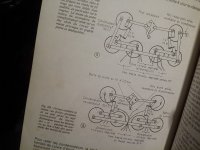
Hello,
Take a look at the attachment. It is all about where the wire '' feeding '' an array of big caps and the wire departing from this array and connect the caps to the should be positioned.
Greetings, Eduard
For those who don't read French, the lower image is more proper, the upper is NG.
Imo, the lower would benefit from a short tab coming off the center point of the ground buss for the ground wire attachment point. To get really fine, you could measure the actual ground current along that ground buss and find the electrical center point - if there is enough current flowing that represents a small improvement.
_-_-bear
Hello,
The French wrote that it does not sound like hum but more like bbbbzzzz when you connect the wires not in the centre of the copper bar but use one of the screw terminal of the caps.
Greetings, Eduard
The French wrote that it does not sound like hum but more like bbbbzzzz when you connect the wires not in the centre of the copper bar but use one of the screw terminal of the caps.
Greetings, Eduard
My suggestion is telling the real experiences instead of the illogical interpretations, and to learn and think basics. In this topic the question is basically wrong. I wrote calculations based on the numbers written here showing the assumptions are false, but it has lost before submitting. I suggest using thompson equation and drawing a sch that contains at least the elements mentioned. But in the end the result will be that there is no resonance at the place it was suspected, so nothing to avoid in this particular case.Suggest making some suggestions?
This is a DIY forum, not a forum for Electronics Engineers, so the idea is to help, and foster learning - the simulation of these things is an "advanced topic" - remember many who read the thread know less than those posting to ask the questions, everyone benefits from good information.
_-_-bear
Pafi, it seems you are a trained EE?
When you throw out the term "Thompson Equation" do not expect that even a majority of people will know what you are talking about. Yes, it is a good thing that we can go and do a search. But a few words of extra explanation as to what the Thompson Equation" illustrates, serves to improve understanding.
Merely telling the OP that he is wrong doesn't really help anyone.
The OP cited a long thread (I have not read it) where apparently this issue is discussed. In a paper many years back Cherry cited situations where there were measurable and unintended HF artifacts due to things like circuit layout, iirc.
_-_-bear
So, I think that Pafi is talking about Lord Kelvin??
https://en.wikipedia.org/wiki/LC_circuit
but likely not gaseous changes due to vapor pressure?
or the thermoelectric effect?
perhaps it is this?
www.nobelprize.org/nobel_prizes/physics/.../1937/thomson-lecture.html
Confusing...
https://en.wikipedia.org/wiki/LC_circuit
but likely not gaseous changes due to vapor pressure?
or the thermoelectric effect?
perhaps it is this?
www.nobelprize.org/nobel_prizes/physics/.../1937/thomson-lecture.html
Confusing...
So, I think that Pafi is talking about Lord Kelvin??
https://en.wikipedia.org/wiki/LC_circuit
Yes, William Thomson, 1st Baron Kelvin, but for me the interesting pont is only the well known formula f=1/(2*pi*sqrt(L*C)). Since the topic is about electrical resonance. This should be the information No 1 to mention and use of course.
Sorry, I spelled wrong, not Thompson, but Thomson, and formula, not equation. I'm not perfect in English.
https://www.google.hu/search?q=thom...hUKEwim6r7K0NzMAhXKORQKHQ-WACIQsAQIJg&dpr=0.9
Pafi, it seems you are a trained EE?
Yes, however I learned thompson formula in secondary school. And anybody who deal with network reactances must know it. Maybe not from the name, maybe only the formula. I wrote it first, but that post has lost.
Merely telling the OP that he is wrong doesn't really help anyone.
I didn't do that. I asked for correct information about the real facts.
The OP cited a long thread (I have not read it) where apparently this issue is discussed.
But in reality it's a different issue from the one described here. This is the reason why I asked what I asked.
I hate rule of thumbs (because some people try to use them over the correct rules), but I share one useful here:
Parasitic HF behaviour of a PCB track or plane pair (which is a distributed network) can be described well by a concentrated capacitor if the surrounding impedance is much higher than the characteristic impedance (Z0), and by a coupled inductance pair if surrounding impedance is much lower than Z0. Here the surrounding impedance is very low (capacitors, n*0.01... n*0.1 Ohm, while Z0 is n*1 ohm), so inductance must be considered, capacitance is negligible.
Parasitic HF behaviour of a PCB track or plane pair (which is a distributed network) can be described well by a concentrated capacitor if the surrounding impedance is much higher than the characteristic impedance (Z0), and by a coupled inductance pair if surrounding impedance is much lower than Z0. Here the surrounding impedance is very low (capacitors, n*0.01... n*0.1 Ohm, while Z0 is n*1 ohm), so inductance must be considered, capacitance is negligible.
This is a DIY forum, not a forum for Electronics Engineers,
Yes. But the question asked in this topic is related strongly to engineering. It's not my fault (if it was a fault). I didn't start it, and didn't ask to do any simulation. But If there is any, then why not to do it with common sense at least?
I would suggest having a look at how the grounding is done on a commercial amp like this:
2016 Assembled Black Box ?Clone Naim NAP200 Amplifier board DIY amp 75W+75W L | eBay
Whatever you might think about Naim, they have most certainly spent some time thinking about grounding and layout. I think it's interesting to note the rejection of most design techniques employed by DIY enthusiasts e.g.:
- OTT brute force 1" thick copper busbars
- Welding apparatus build
- Ultra compact pcb layout
- Electrically separate channels (although this is probably dictated by their overall system grounding scheme)
- Local decoupling and by passing
- Ground planes and multilayer boards
Worth some thought???
I would suggest having a look at how the grounding is done on a commercial amp like this:
2016 Assembled Black Box ?Clone Naim NAP200 Amplifier board DIY amp 75W+75W L | eBay
Whatever you might think about Naim, they have most certainly spent some time thinking about grounding and layout. I think it's interesting to note the rejection of most design techniques employed by DIY enthusiasts e.g.:
- OTT brute force 1" thick copper busbars
- Welding apparatus build
- Ultra compact pcb layout
- Electrically separate channels (although this is probably dictated by their overall system grounding scheme)
- Local decoupling and by passing
- Ground planes and multilayer boards
Worth some thought???
Also to be considered is the specific specifications of the amplifier.
For example the people at Spectral when they made the DMA-50 and DMA-100 had to work very hard to make that amp work out to the bandwidth they wanted. So their techniques perhaps reflected different techniques than the Naim board which has modest specs in terms of slew rate, rise times, current capability, etc...
Btw, no one uses 1" thick copper buss bars, perhaps 1" wide? 😀
I could only find one 400A diode that might call itself HEXFRED: datasheet here. What part number of 400A diodes did you use back in 1991?
Mark,
I made a mistake. They are 400V and mere 90 amp:
VISHAY
HFA90NH40 Series 400V 240 ns Ultrafast Soft Recovery Rectifier - HALF-PAK (D-67)
It's been 20+ years... 😱
Paci, Bear, DF96, OS, Infinia, Eduard, Conrad and David,
Thank you very much for posting and helping me (and other newbies) to learn and understand the problems. I am sorry that for the past weekend I was fully occupied and didn't have time to check the forum or do any soldering / measurements. Having 3 teens and a wife and a full time job doesn't allow me to have as much time as I would like doing my favourite thing - audio DIY.
Please keep up your good work and I will respond in due time (I am currently stealing a couple of minutes from work at lunch time to respond).
Regards,
Bill
Wow, my amp now sounds better!
Last Sunday I found some time to do a mod to the PSU of the amp. Based on your advice I was trying to reduce the PSU DC impedance to see if it was going to improve on the sound.
I reduced the CLRCLRCLRC to CLRC using exactly the same number of small capacitors on the board by shorting out some LRs. That is,
From 8160uF - 1uH - 0.22R - 2720uF - 1uH - 0.22R - 2720uF - 1uH - 0.1R - 12240uF
To 8160uF - 1uH - 0.1R - 17680uF
After 2 nights of music listening I believe the amp is now more musical with less distortion. It appears to be the case that the harshness I described earlier has been reduced to at least half. It is a welcoming improvement.
So what was helping with the improvement? Was it the DC impedance? When the rectifier diodes are conducting, the DC impedance reduction was from 0.54R to 0.1R, with the transformer secondary winding resistance being 0.18R. When the diodes are not conducting, the impedance is still better with the CLRC than the CLRCLRCLRC because the last C is 44% larger.
What do you think of getting rid of the last LR (1uH - 0.1R)? Would it make it better or worse?
Which do you prefer? 8160uF - 1uH - 0.1R - 17680uF or a single C of 25840uF?
I have not had time to do any measurements.
Simulations seem to suggest that 8160uF - 1uH - 0.1R - 17680uF should be a lot better than 25840uF alone. But I can be wrong. I previously thought CLRCLRCLRC was better than CLRC and I was wrong.
Simulations seem to suggest that 8160uF - 1uH - 0.1R - 17680uF should be a lot better than 25840uF alone. But I can be wrong. I previously thought CLRCLRCLRC was better than CLRC and I was wrong.
My first guess is that the increase of 40% in the last C is the main cause of the change.
It is possible that the 7pole filter was resonating, but with all that resistance it should have been damped.
It is possible that the 7pole filter was resonating, but with all that resistance it should have been damped.
The 1uH inductors will not do very much, so they can be omitted. At best, they isolate the earlier capacitors from the AC load current at higher audio frequencies. They don't contribute to smoothing as they are too low in value for this. They don't filter out RF as the electrolytics won't have a low impedance at RF frequencies. Essentially you just have a distributed slightly lossy capacitor. 0.54R is quite high an impedance for a power amp supply.HiFiNutNut said:From 8160uF - 1uH - 0.22R - 2720uF - 1uH - 0.22R - 2720uF - 1uH - 0.1R - 12240uF
8160uF fed at 100Hz will have an effective DC impedance of 0.6R, so you have a total DC impedance of around 1R. Get rid of (most of) the series resistance and then all the caps can work in parallel. Total of 25840uF has an effective DC impedance of 0.2R: five times better. By 'DC' I also include low audio and subsonic - basically anything significantly below 100Hz.
There is a reason why traditionally an audio power amp just used a big electrolytic in the PSU, and designed the amp for good PSRR.
- Status
- Not open for further replies.
- Home
- Amplifiers
- Solid State
- Capacitor Array on Power and Ground planes – How to Avoid Resonance?