We want low impedance power supply at AF as well as at RF.
The old trick was to parallel film / ceramic caps with electrolytic caps but modern electrolytic caps have low ESR and low ESL therefore can work pretty well themselves. They don’t require paralleled film / ceramic caps, the latter of which can cause impedance peaking / resonance due to LC resonance formed between PCB tracks and internal LCR of the low impedance capacitors. This has been covered in lengthy discussions in the past and I have learnt a great deal from them.
On the other hand, having read from a lot of posts about the benefits of capacitor array on power and ground planes I have experimented rebuilding my preamp and power amp with such power supplies – having some copper zones (small or large) of local power and ground planes on the PCBs with numerous smaller value low ESR and low ESL capacitors on them up close to the active devices they power. I thought that the power and ground planes provide very low inductance current path and along with multiple low ESR low ESL capacitors they provide a very low impedance power supply. But so far the result has not been positive. I can measure low level resonance in the tens of MHz region. The resulting amplifiers sound worse than before.
I have limited measurement capability and limited knowledge hence my question here. But I have just thought of one thing I did not think of – the power and ground planes on which the cap array is built possibly form a small value, very low ESR, very low ESL, very high Q capacitor! (or does it?) Using a simple LCR meter I measured from 200pF to 1.2nF capacitance between the planes. So my guess is that this high Q capacitor formed by the planes reacts to the LCR of the low impedance cap array, the scenario is exactly the same as paralleling film / ceramic capacitors with low ESR capacitors in our old trick! Or not?
Of course, I can be completely wrong. I am here to learn. If you have working experience and knowledge please help me to understand the issue and find a solution. Perhaps I should keep the ground plane but ditch the power plane?
Last edited:
The devil's in the detail here - please share pics/schematics of where you've used multiple paralleled caps and gotten worse sound. Perhaps there's some sub-optimal wiring arrangement you've used - with very low impedance capacitor arrays the currents can be rather high and this means the wiring topology becomes that much more critical.
low Z from DC to light on a PS is silly, why are you asking for it?
large area single layer caps on FR4 make lousy RF capacitors low Q and highly resonant.
RF and audio circuits benefit more from local decoupling using a series element, targeting the frequencies involved. Look at it from the system (bigger) picture 1st. don't throw all your problemos over the wall to poor PS guys. BTW often big power planes need cuts and slices to isolate noise from being injected into "ground" creating common mode noise> people that specify ground planes for audio are dummies and the PS guys do it mainly for current density not RF.
Last edited:
I will post some pictures when I can get to my home computer.
Without a ground plane the return path for local decoupling would be on a PCB track back to a local star ground, and that is fairly inductive. In that case would the local decoupling be still effective?
Without a ground plane the return path for local decoupling would be on a PCB track back to a local star ground, and that is fairly inductive. In that case would the local decoupling be still effective?
Fairly inductive ? Nano henries ... ?
With wider traces on an output stage , still nH.
At a higher Z node (and a 1mm trace) - like at the VAS base and Cdom ,
a ground plane will add about 3pf - inch / 1pf - cm. No good.
I don't do any ground planes for analog. Adds too much stray C.
Short high Z traces and short symmetrical ground returns.
Most CAD's will not design audio right , they are set up for digital.
Here - https://www.google.com/url?sa=t&rct...sg=AFQjCNHLctfFjfF5eBPKA07n3SfSwn1_Vw&cad=rja
TI 's "take" on this issue ....
OS
Last edited:
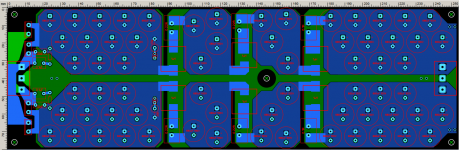
Finally, this is a prototype multi-stage line level active crossover board. It is in a 4 layer FR4.
The negative plane and ground plane forms a 1.2nF capacitor (0.175mm distance). The positive plane and the ground plane forms a 200pF capacitor (1.13mm distance).
It makes provisions for having some 0.1uF X7R SMD on each opamp power pin and some electrolytic capacitors.
The negative plane and ground plane forms a 1.2nF capacitor (0.175mm distance). The positive plane and the ground plane forms a 200pF capacitor (1.13mm distance).
It makes provisions for having some 0.1uF X7R SMD on each opamp power pin and some electrolytic capacitors.
Attachments
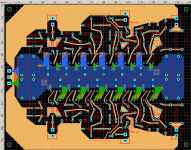
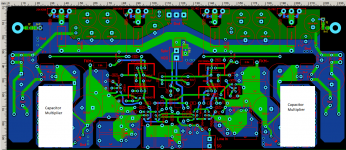
Here is the prototype amplifier board. It made provisions for some 1uF MKP to bypass small electrolytic caps. The MKPs are not installed.
On the top side is the local power supply with small zones of ground and power planes. The ground plane also covers the LMOSFET output tracks. On the left and right sides are 2 capacitor multipliers that have quiet output and low output impedance (0.05R or so). In the middle part are the IPS and VAS that are not covered by planes.
P.S. Sorry I deleted the first posted message and recreated it here as I realized that I should remove the part labels of the capacitor multipliers on the image because the schematic was a friend's gift and I need to protect his copyright. The amplifier schematic is OK because it was in the public domain.
Attachments
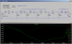
the series resistors are real resistors or there to model the series resistance of your inductors??
Is this for a low level circuit or power amp?
The "resonance" you are seeing probably does not exist in reality, but you can explore it in SPICE by moving the exciting frequency range (the source on the left of the schematic) to a bandpass closer to the area of interest.
What ur seeing looks like some sort of notch type filter, which may be an artifact of the parameters for your caps and inductors - which may not really exist in a real circuit since the series reactance of both the caps and inductors may roll off much faster than the "perfect" spice models show.
Also, what is the purpose of this filter, it does not do a good job at low frequencies?
If you want to design an effective filter up at RF freqs to get <~80db supression (ie. get near to the ambient RF noise floor - in most environments) you'll need to do more than stack multiple filters in series, you'll need to look at RF design techniques too.
Also the series R of your supply makes for a relatively high impedance current source for a power amp. Also most power amps will have sufficiently high PSRR to kill all the stuff ur worried about, AND they will not have any amplification at 10mhz that is meaningful. Do you have a power amp design that gets any where near -100dB down for IM & THD?
And, is or was there a problem that you're trying to solve with this??
Another thought... if you simplify to a 3rd or 4th order filter and muck about with the values, changing the Q, I think you will find that a LP filter will end up with significant peak/ripple before the rolloff, you may be seeing that simulated in SPICE since it looks at the entirety of your stacked LP sections as a single filter...
_-_-
_-_-
the series resistors are real resistors or there to model the series resistance of your inductors??
Is this for a low level circuit or power amp?
The "resonance" you are seeing probably does not exist in reality, but you can explore it in SPICE by moving the exciting frequency range (the source on the left of the schematic) to a bandpass closer to the area of interest.
What ur seeing looks like some sort of notch type filter, which may be an artifact of the parameters for your caps and inductors - which may not really exist in a real circuit since the series reactance of both the caps and inductors may roll off much faster than the "perfect" spice models show.
Also, what is the purpose of this filter, it does not do a good job at low frequencies?
If you want to design an effective filter up at RF freqs to get <~80db supression (ie. get near to the ambient RF noise floor - in most environments) you'll need to do more than stack multiple filters in series, you'll need to look at RF design techniques too.
Also the series R of your supply makes for a relatively high impedance current source for a power amp. Also most power amps will have sufficiently high PSRR to kill all the stuff ur worried about, AND they will not have any amplification at 10mhz that is meaningful. Do you have a power amp design that gets any where near -100dB down for IM & THD?
And, is or was there a problem that you're trying to solve with this??
Thanks for your reply.
The resonance I referred to is not the resonance in the LTSpice model, but measured resonance (very mild) using a 150MHz scope with 2mV Div running on battery. I suspect that the resonance comes from the power and ground planes forming a small value low ESR high Q capacitor resonating with the low ESL electrolytic capacitor array.
Good questions about the R of the power supply. The power supply is for a power amp. I was hoping that CLRCLRCLRC will get rid of most noise from the mains as well as from the rectifier switching noise. Because the IPS and VAS rail is "regulated" with a low noise low output impedance capacitor multiplier, the power supply schematic shown is only for the OPS stage which has a high PSRR at low frequencies. It is for this reason I think a slightly higher impedance (at low frequencies) PSU of CLRCLRCLRC should work.
When the rectifier diode is turned on, the AC source impedance is 0.5R and the CLRCLRCLRC adds another 0.54R. So at low frequencies the current generated noise is about 6dB difference. When the rectifier diode is turned off, or at higher frequencies there is basically no difference because in that case only the last C counts, and the last C has 12,000uF+ capacitance.
A classic newbie mistake is to cascade lots of PSU smoothing sections in order to achieve the perfect low noise PSU. It might work in simulation. The usual result in real life is buzz from poor grounding, and LF instability due to unwanted subsonic feedback via the PSU impedance.
I would not worry about a supposed very mild VHF resonance in an audio PSU. Unless you are an experienced RF engineer it is likely that all you are seeing is broadcast pickup, not a real resonance. If you were an experienced RF engineer you would not need me to tell you this.
I would not worry about a supposed very mild VHF resonance in an audio PSU. Unless you are an experienced RF engineer it is likely that all you are seeing is broadcast pickup, not a real resonance. If you were an experienced RF engineer you would not need me to tell you this.
We want low impedance power supply at AF as well as at RF.
<snipage>
Of course, I can be completely wrong. I am here to learn. If you have working experience and knowledge please help me to understand the issue and find a solution. Perhaps I should keep the ground plane but ditch the power plane?
wait, assume somehow you managed to make a perfect Voltage Source DC-Light, as soon as you hook it to a couple of power amps driving a decent load you will still measure ripple at the amps PCBs. hmmmm... confusing and a waste of effort.
Here is my power amp PSU schematic.
your model assumes a perfect ground (1st big mistake) not a valid assumption at high currents on a PCB with ground plane. But wait your system still has a real ground to consider > the earth connection ( ANY time you make a real noise / ripple measurement it is referenced to earth) / also wires and real transformers exist to hook up to your PCBs those must be modeled. After you model all that, comes the linear ripple analysis from both ends> the line related and load related. Then for extra credit the non linear analysis comes next, the rectifiers and output devices.
Last edited:
Thanks for your reply.
The resonance I referred to is not the resonance in the LTSpice model, but measured resonance (very mild) using a 150MHz scope with 2mV Div running on battery. I suspect that the resonance comes from the power and ground planes forming a small value low ESR high Q capacitor resonating with the low ESL electrolytic capacitor array.
<snip>
Ok, so shoot a screen shot of your scope and post.
Let's see the bugger!
You did not answer if the R in the SPICE model represents actual real physical resistors or the modeled DCR of components??
The <2mV things you are seeing, how do you know they are being produced by the circuit?
Steady state at quiescent (no signal)?
Dynamic, run with a load and signal??
Turn the amp off, it goes away?
And I did not understand your comment on the filtering, you say the LAST filter cap is large?? (generally speaking that is "backwards")
...I can measure low level resonance in the tens of MHz region.
How have you measured this?
the power and ground planes on which the cap array is built possibly form a small value, very low ESR, very low ESL, very high Q capacitor! (or does it?)
Probably not. FR4 is not a low loss dielectric, it's not optimized for capacitor use, after all.
Best wishes
David
I think he is saying that the "sandwich" is creating an undesired capacitance, which is contributing to the presumed unwanted "resonance"...
... the "sandwich" is ...an undesired capacitance...
Yes, I understand this, my point is that FR4 board substrate is a fairly lossy dielectric so the Q would not be hi, as he claims.
Best wishes
David
- Status
- Not open for further replies.
- Home
- Amplifiers
- Solid State
- Capacitor Array on Power and Ground planes – How to Avoid Resonance?