Trying to measure the residual distortion of L-R, what do you recommend? A center tapped trafo would be good.
If you have a QA403, use the differential in. With a scope, use math.
Thor

Sorry @fabrice63 for late reply. I missed this one.Interresting , what do you think will be the issues having a to quick slew rate ?
I was informed that:
"faster than necessary" flanks
and
"higher amplitude than necessary"
signals
will cause noise contamination in substrate which will leak globally to the entire chip (shows up at the output + affect other functional blocks).
"Stopped clock" operation eliminates BCK related noise (great idea) at the moment of conversion (when it matters most), but does not eliminate other contaminants.
I implemented stopped clock operation + Slew Rate attenuators, but sonically it was equivalent to not using stopped clock at all (no sonic benefit) - something that others appear to have also noticed.
I would say it is a really great idea, but attenuators lead to better objective and subjective results.
Cheers
I was informed that:
"faster than necessary" flanks
and
"higher amplitude than necessary"
signals
will cause noise contamination in substrate which will leak globally to the entire chip (shows up at the output + affect other functional blocks).
Yes. The input transistors are PNP in a specific technology, that creates a lot of capacitance to the substrate.
The PNP transistors load with a resistor from emitter to +5V and most likely connect the collector for to -5V.
There is another NPN transistor that follows, collector to +5V, level shifter diode chain in the emitter also with emitter resistor to -5V. After that is a standard CML/ECL input for CML/ECL(ogic) between DGND and -15V.
Very standard for late 1980's high speed circuitry.
The circuit creates several problems.
Currents flow in +5V & -5V from these input circuits. The greater the input swing, the greater these current. This is likely the reason why HtP insisted on a direct RF decoupling path between +5V and -5V.
Internal clamping limits the swing at input PNP transistor emitter to 0.6V...2.4V for 0V to 1.8V (temperature dependent) input. At higher input (than ~ 1.8V), the Input PNP transistor reverse biased, meaning to will be slow to react to a falling edge.
The best range for the input, if my "TTL 2 ECL" hypothesis is right, is around 0.9V to 1.8V, which matches well with practical observation. Using 1.8V CMOS logic (74AUCXX) for re-clocking would be one option to allow a simple series resistor to form the sole signal conditioning circuit.
The high capacitance from the input transistor base to substrate (~12pF) causes fast edges to couple into the substrate, which forms a bulk resistance of tens of Ohm to -15V.
All NPN transistors in the IC sit on this substrate, so noise there is coupled back into the entire output DEM circuit. So it appears at the output.
At the same time, as all logic baring the input is differential all the way to the bit switches, the logic is pretty much unaffected by the noise in the substrate.
Only the leakage of the edges into the audio output are of real concern.
"Stopped clock" operation eliminates BCK related noise (great idea) at the moment of conversion (when it matters most), but does not eliminate other contaminants.
The above is an urban legend. There is no "moment of conversion" where removing the mainly BCK and Data related noise matters.
It is likely still an improvement, as typically stopped clock uses a higher frequency for BCK than needed, causing other potential issues, but being easier to filter.
And the period during which this easier to filter noise exists is only 50% or less of the time. So any process using averaging (e.g. FFT) will show improvements.
If no signal conditioning is used and especially if the source is modern CMOS logic with very high edge rates, stopped clock can provide objective and likely subjective improvements, but it is preferred to use correct signal conditioning instead.
Thor
From page 8 of the PMD100 datasheet.The above is an urban legend.
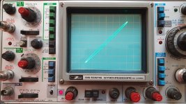
I can't understand what I see on the picture. X=L, Y=R, there is some phase difference (20 us or so), but why? Freq 440 Hz, I/V is DC coupled.
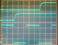
The conversion does not happen at the same time in both channels? The difference seems in the order of 1 WS time.
The conversion does not happen at the same time in both channels? The difference seems in the order of 1 WS time.
Attachments
With TDA1543, there is a delay of 1 bitclock period between L and R output.
With TDA1543A, output is simultaneous as far as I could observe in my scope. Same for TDA1545.
Never tested this with TDA1541.
With TDA1543A, output is simultaneous as far as I could observe in my scope. Same for TDA1545.
Never tested this with TDA1541.
I can't understand what I see on the picture. X=L, Y=R, there is some phase difference (20 us or so), but why? Freq 440 Hz, I/V is DC coupled.
The conversion does not happen at the same time in both channels? The difference seems in the order of 1 WS time.
How do you determine if there is a time difference if the X axis is no longer time?
I'm not that experienced with X-Y mode. But I think you are misinterpreting this.

I can't understand what I see on the picture. X=L, Y=R, there is some phase difference (20 us or so), but why? Freq 440 Hz, I/V is DC coupled.
IIS input or SIM?
Thor
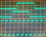
Strange, this is always like 1 WS cycle difference in with I2S format of input datas?
Should be checked for TS format of input datas and compare?
...
Sorry for asking did You check 3 option pin input format set?
Should be checked for TS format of input datas and compare?
...
Sorry for asking did You check 3 option pin input format set?
Last edited:
No. Data of both left and right should be latched when BCK goes up after WS has gone down.Perhaps normal, this is how Word Select works.
According to the I2S bus specification (see attached), R channel is latched when WS is high, and L channel is latched when WS is low, on the next leading edge of the SCK. That means 1/2 WS period, but I measured a full WS period between the channels.No. Data of both left and right should be latched when BCK goes up after WS has gone down.
If there is time difference between the channels, be it 1 WS period or 1/2, simultaneous mode looks better.
In my test pin 27 is connected to pin 28, this should select time multiplexed 2s complement format.
Attachments
Probably?Then perhaps the i2s.h library in my Arduino code has some flaw.
Do You have some other I2S source?
Did You try with higher WS (SR) maybe, to chect does it still 1xSR time?
- Home
- Source & Line
- Digital Line Level
- Building the ultimate NOS DAC using TDA1541A