Lt1166
Hmm.... there a few things I don't understand:
1. C14=1F across pin 1 and 4. Doesn't this quite large cap spoils the control function?
2. The idle drain current is ~90mA, that means that the product is 8100E-6. So how on earth can it peak at 400E-6?
Perhaps (and if time allows) you may check/simulate Id figures of the complete amp (or at least the OPS) you have once built with this chip, because I'm not sure if the circuit you just simmed is appropriate to examine the discrepancy that I've observed.
Edmond Stuart said:Hmm.... there a few things I don't understand:
1. C14=1F across pin 1 and 4. Doesn't this quite large cap spoils the control function?
2. The idle drain current is ~90mA, that means that the product is 8100E-6. So how on earth can it peak at 400E-6?
Perhaps (and if time allows) you may check/simulate Id figures of the complete amp (or at least the OPS) you have once built with this chip, because I'm not sure if the circuit you just simmed is appropriate to examine the discrepancy that I've observed.
1. Maybe in AC, but shouldn't the loop act at DC only? That's why I was asking about any possible frequency effects.
2.
90mA*90mA=90,000uA*90,000uA=8.1*10^9 uA^2
I got Id(M1)*Id(M2)=400 uA^2
Edit: I have just tried 100uF and it's still 400uA^2. However, at 1uF it's 75mA^2! So that's definitely a frequency issue.
LT1166
DC only? I don't thinks so, as the data sheet describes this chip as "A high speed regulator loop [that] controls the amount of drive applied to each power device." To me, that means it's intended to be active throughout the whole audio spectrum.
Furthermore, their 100W amp, fig. 19, has no cap between pin 1 and 4.
Last but not least, such cap will spoil the whole concept as it will be charged to a higher voltage under dynamic condition, resulting in an increase of the bias level.
Okay, the math is correct, but I consider that 400 uA^2 as a dip instead of a peak as the base line is much higher (8.1*10^9 uA^2).
So, in order to compare our results, I'm afraid you will need another test circuit.
BTW, may we have a look at the schematic of your amp?
syn08 said:Maybe in AC, but shouldn't the loop act at DC only? That's why I was asking about any possible frequency effects.
DC only? I don't thinks so, as the data sheet describes this chip as "A high speed regulator loop [that] controls the amount of drive applied to each power device." To me, that means it's intended to be active throughout the whole audio spectrum.
Furthermore, their 100W amp, fig. 19, has no cap between pin 1 and 4.
Last but not least, such cap will spoil the whole concept as it will be charged to a higher voltage under dynamic condition, resulting in an increase of the bias level.
90mA*90mA=90,000uA*90,000uA=8.1*10^9 uA^2
I got Id(M1)*Id(M2)=400 uA^2
..............
Okay, the math is correct, but I consider that 400 uA^2 as a dip instead of a peak as the base line is much higher (8.1*10^9 uA^2).
So, in order to compare our results, I'm afraid you will need another test circuit.
BTW, may we have a look at the schematic of your amp?
Re: LT1166
I don't know. Originally I used it myself without the cap (see below), eventually I added a 1u cap and it worked slightly better (less HF distortions).
http://www.diyaudio.com/forums/showthread.php?postid=1107005#post1107005
Edmond Stuart said:
DC only? I don't thinks so, as the data sheet describes this chip as "A high speed regulator loop [that] controls the amount of drive applied to each power device."
BTW, may we have a look at the schematic of your amp?
I don't know. Originally I used it myself without the cap (see below), eventually I added a 1u cap and it worked slightly better (less HF distortions).
http://www.diyaudio.com/forums/showthread.php?postid=1107005#post1107005
I hope you still have that schematic on your PC. With that one (without cap) it's quite easy to verify my results.
I agree with you, with a 1uF cap one gets less HF distortion, because it reduces the bias voltage modulation. But, as already mentioned, there are some unwanted side effects.
In the mean time I've figured out why this chip has a pos. TC. The reference current source (around Q42) is the culprit. Whether this was done intentionally, we will probably never find out.
PS: Our posts were crossing!
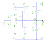
syn08 said:I modified the schematic as in the attachment. Now, with C14=1pF Id(M1)*Id(M2) is still 400uA^2
This setup is unsuitable for a Id(M1)*Id(M2) test, because pin 1 and 4 are still (AC wise) shorted by C15 and C16. In a couple of hours I will drop a version without that short.
edit: Here it is already:
Attachments
Edmond Stuart said:
This setup is unsuitable for a Id(M1)*Id(M2) test, because pin 1 and 4 are still (AC wise) shorted by C15 and C16. In a couple of hours I will drop a version without that short.
edit: Here it is already:
This is a closed loop configuration with a gain of one. I'm not sure if this configuration is valid, LT recommends other ways to close the loop (and avoid using the transconductance stage at pin 2).
http://www.linear.com/pc/downloadDocument.do?navId=H0,C3,P1163,D5943
I'll take another look myself. But I'm also not sure why using the LT1166 in "DC mode" is a problem. I did it and found no practical issues.
Edmond Stuart said:
As I said before, "such cap will spoil the whole concept as it will be charged to a higher voltage under dynamic condition, resulting in an increase of the bias level."
It's not about the gain, it's about closing the loop that way.
I must be dense today, but I fail to understand what you are talking about. How would this "increase in bias level" manifest? And how would this "increase in bias" be different from a standard Vbe multiplier?
I did exactly that and I have not noticed any adverse effects.
Edit: Whoops, your post just vanished.
syn08 said:This is a closed loop configuration with a gain of one. I'm not sure if this configuration is valid, LT recommends other ways to close the loop (and avoid using the transconductance stage at pin 2).
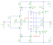
Okay, here is an example with a gain of 31. Regarding the behavior of the bias loop, I observed no differences.
I'll take another look myself. But I'm also not sure why using the LT1166 in "DC mode" is a problem. I did it and found no practical issues.
As I said before, "such cap will spoil the whole concept as it will be charged to a higher voltage under dynamic condition, resulting in an increase of the bias level."
With 100uF and at 10kHz, the bias will rise from an initial 148mA to 180mA after a couple of cycles. Okay, in practice not a serious issue, but this chip was designed NOT to do such things. Instead, it should hold the bias at a constant level.
When examining the loop behavior (the product of Id's, for example), this cap should be removed, otherwise one will get completely erroneous results.
edit: Oops, posts were crossing
Attachments
You may close the loop in any other way. Does it really matter? No!
Observe the voltage of that cap with a value of 0 resp. 100uF under dynamic conditions, that is, large excursions of the OPS. With 0uF the voltage will increase -on purpose- when the OPS delivers large currents to the load. With a large cap, this thing will hold that charge (and voltage). As a result..... guess what.
>different from a standard Vbe multiplier?
Yes, simply, because this thing does keep bias voltage constant.
Well, I am not so sure. Have you tried the LT recommended schematic I've posted a link to?Edmond Stuart said:You may close the loop in any other way. Does it really matter? No!
Honestly, as long as it does not have an impact on the performance (and I don't see how even 20% increasing the bias would) I couldn't care less about this effect. BTW, I was not able to measure such a bias increase effect (the measured bias was always rock solid).
LT1166
No. Why should I, as it doesn't matter?
Whether you care (or don't care) about a 20% increase of the bias is beside the point. And if you were not able to measure such a bias increase effect, you may look (or think) a bit harder.
(BTW, if you don't care, just use an ordinary Vbe multiplier 🙂)
The point is that this chip (or the model, but probably both) does not perform as promised by the data sheet.
syn08 said:Well, I am not so sure. Have you tried the LT recommended schematic I've posted a link to?
No. Why should I, as it doesn't matter?
Honestly, as long as it does not have an impact on the performance (and I don't see how even 20% increasing the bias would) I couldn't care less about this effect. BTW, I was not able to measure such a bias increase effect (the measured bias was always rock solid).
Whether you care (or don't care) about a 20% increase of the bias is beside the point. And if you were not able to measure such a bias increase effect, you may look (or think) a bit harder.
(BTW, if you don't care, just use an ordinary Vbe multiplier 🙂)
The point is that this chip (or the model, but probably both) does not perform as promised by the data sheet.
Re: LT1166
To me, as long as you don't use this chip as recommended by the manufacturer, you do not have a valid point. You may though want to write LT and tell them about your findings.
According to my measurements, if used properly, this little chip is an excellent $2 and 0.05 sq. in. MOSFET bias helper.
Over and out.
Edmond Stuart said:
The point is that this chip (or the model, but probably both) does not perform as promised by the data sheet.
To me, as long as you don't use this chip as recommended by the manufacturer, you do not have a valid point. You may though want to write LT and tell them about your findings.
According to my measurements, if used properly, this little chip is an excellent $2 and 0.05 sq. in. MOSFET bias helper.
Over and out.
malicious obstruction
In essence, I did exactly what LT has recommended, i.e. feeding pin 1 and 4 four by current sources and NOT putting a large cap between these two connections. As long as you refuse to understand that and showing a total unwillingness to grab my point (to put it mild), it's indeed better to close down this unfruitful discussion.
syn08 said:To me, as long as you don't use this chip as recommended by the manufacturer, you do not have a valid point. You may though want to write LT and tell them about your findings.
According to my measurements, if used properly, this little chip is an excellent $2 and 0.05 sq. in. MOSFET bias helper.
Over and out.
In essence, I did exactly what LT has recommended, i.e. feeding pin 1 and 4 four by current sources and NOT putting a large cap between these two connections. As long as you refuse to understand that and showing a total unwillingness to grab my point (to put it mild), it's indeed better to close down this unfruitful discussion.
Re: Where complementary symmetry and traditional miller compensation rules supreme.
Hi Brian,
I apologize for bringing up the questions so late, but I was away on vacation and am finally catching up with some of the posts.
Your amplifier looks very interesting and your post brings up some good topics to discuss. There are certainly interesting challenges in driving 20 pairs of output transistors! Congratulations on such an ambitious project.
I have a couple of questions, partly because I can’t read some of the component values on the schematic.
Two big things that limit slew rate are the ability of the input stage to charge the Miller compensating capacitor and the ability of the VAS to charge the load capacitance. You correctly point out that the complementary architecture you have shown can, under the right conditions, enter class-B operation and deliver more than double its standing current to charge the output stage load capacitance. It is true that the unipolar input stage arrangements that I like usually cannot do that (enter class B), or don't do it very well.
It looks like your waveforms show at least 300 V/us without the added output stage capacitive load, but only about 100 V/us with the 1000 pF output stage load. This seems to be reasonably consistent with the 110 mA peak current that you said the VAS could deliver in its class B mode of operation. Is that correct, or am I missing something?
In order to achieve 300 v/us, it looks like each half of the input stage needs to be able to deliver about 9 mA to its respective 30 pF Miller compensation capacitor. Does this mean that your input-pair tail currents are something in excess of 9 mA?
What value emitter degeneration resistors did you use in the input pairs and what is the closed-loop gain of the amplifier?
If the complementary input pairs are running at more than 9 mA, is that why you elected to precede them with a JFET CFP buffer on each side?
What is the input-referred noise of the amp?
I understand your concern about adding a fourth level of emitter follower stage to the output stage. We all have to pick our poison in such a challenging situation. Nevertheless, it seems pretty cruel to load a VAS with 1000 pF of nonlinear junction capacitance (I realize the MJ15030 may not actually be that bad). I would have put a folded emitter follower in front of the Triple, or used a Diamond buffer as the first two stages of buffering. That way, the Vbe’s don’t add up so badly. Then you could have run the VAS at only 10 mA and would never need it to go class-B to achieve high slew rate. Just a different design choice; we don’t always pick the same poison.
Cheers,
Bob
G.Kleinschmidt said:Hi Ho
I’m now in the final design/construction stages of my K800AB amplifier.
Since my last postings detailing the full complementary / symmetry front-end design that is capable of slewing ~300V/us and ~600V/us when miller compensated for unity loop gain frequencies of 1MHz and 2MHz respectively, I have made a few revisions.
These stemmed from the difficulty in driving the massive output stage.
The output stage consists of twenty pairs of MJL3281/MJL1302 power transistors divided into five groups of four parallel-connected pairs. Each group of four pairs has its own MJE15032/MJE15033 complementary driver pair, and these five pairs of drivers are driven from a single MJE15030/MJE15031 complementary pair.
The difficulty arises from the fact that the MJE15030/MJE15031 pre-driver pair presents a significant capacitive load. This is especially so when driven at a high slew rate, causing high transient emitter currents to flow.
Driving such a stage directly from the VAS in its previous incarnation would result in a mediocre slew rate at best.
The design required extensive buffering of the VAS from the triple emitter follower output stage in order to achieve a high slew rate. While perfectly doable, this is an inelegant PITA to implement, especially so when it comes to temperature compensating the output stage.
Driving a capacitive load at very high slew rates directly from the VAS collector also causes issues WRT to frequency compensation. Previous experiments to achieve adequate performance with feed-forward compensation were the “miller” compensation capacitor is returned from the VAS collector to the inverting input were less than promising.
The problem was that the “miller” feedback capacitor at ~30pF or so was not the dominant capacitive load on the VAS. Driving a relatively high capacitive load directly from the VAS collector made it difficult to compensate the miller loop (now consisting of the VAS and input long tail pairs combined) for adequate step response free of ringing and ripple.
Then I read this revealing National Semiconductor design brief:
http://www.national.com/appbriefs/files/AppBrief108.pdf
Basically, an properly built amplifier frequency compensated solely with the traditional collector-base miller compensation capacitor will be inherently immune to capacitive loading of the VAS collector, with a perfect, ringing free step response and whistle clean slew rate limiting guaranteed.
National Semiconductor took advantage of this fact in the design of an unlimited load capacitance opamp, by omitting the output stage and driving the output directly from the VAS collector.
So, I went back to the traditional collector-base miller compensation and beefed up my VAS.
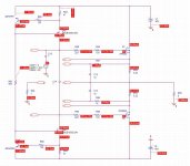
A screen shot of the basic simulation is attached below. In order to achieve a high slew rate into the MJE15030/MJE15031 pre-driver pair, the VAS was trebled up. Quiescent current is 30mA and peak current is limited to +/-110mA.
This is where full complementary circuit topologies rule over unipolar or single ended ones – the VAS can be designed to deliver well over twice its quiescent current into a hefty or difficult to drive load.
For the sole purpose of demonstrating the slewing performance and step response of the VAS, the simulation was simplified with a unity gain VCVS to act as an ideal output stage.
The front-end circuit is simulated twice, driven to an output voltage of 80Vp-p with a 200kHz squarewave. The miller compensation capacitors are selected for a unity loop gain frequency of 1MHz.
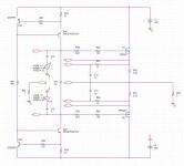
The green trace shows the output voltage of the circuit on the left, which has no additional capacitive load presented to the VAS. The red trace shows the output voltage of the same circuit repeated on the right, but whose VAS collector is loaded to ground with a 1nF capacitor.
Harbuch will have my four 800VA toroids wound in 4 to 5 weeks, soon after which, with any luck, I’ll be in a position to post up some nice squarewave oscillograms made with the dummy load boiling water in a bucket.
Cheers,
Glen
An externally hosted image should be here but it was not working when we last tested it.
Hi Brian,
I apologize for bringing up the questions so late, but I was away on vacation and am finally catching up with some of the posts.
Your amplifier looks very interesting and your post brings up some good topics to discuss. There are certainly interesting challenges in driving 20 pairs of output transistors! Congratulations on such an ambitious project.
I have a couple of questions, partly because I can’t read some of the component values on the schematic.
Two big things that limit slew rate are the ability of the input stage to charge the Miller compensating capacitor and the ability of the VAS to charge the load capacitance. You correctly point out that the complementary architecture you have shown can, under the right conditions, enter class-B operation and deliver more than double its standing current to charge the output stage load capacitance. It is true that the unipolar input stage arrangements that I like usually cannot do that (enter class B), or don't do it very well.
It looks like your waveforms show at least 300 V/us without the added output stage capacitive load, but only about 100 V/us with the 1000 pF output stage load. This seems to be reasonably consistent with the 110 mA peak current that you said the VAS could deliver in its class B mode of operation. Is that correct, or am I missing something?
In order to achieve 300 v/us, it looks like each half of the input stage needs to be able to deliver about 9 mA to its respective 30 pF Miller compensation capacitor. Does this mean that your input-pair tail currents are something in excess of 9 mA?
What value emitter degeneration resistors did you use in the input pairs and what is the closed-loop gain of the amplifier?
If the complementary input pairs are running at more than 9 mA, is that why you elected to precede them with a JFET CFP buffer on each side?
What is the input-referred noise of the amp?
I understand your concern about adding a fourth level of emitter follower stage to the output stage. We all have to pick our poison in such a challenging situation. Nevertheless, it seems pretty cruel to load a VAS with 1000 pF of nonlinear junction capacitance (I realize the MJ15030 may not actually be that bad). I would have put a folded emitter follower in front of the Triple, or used a Diamond buffer as the first two stages of buffering. That way, the Vbe’s don’t add up so badly. Then you could have run the VAS at only 10 mA and would never need it to go class-B to achieve high slew rate. Just a different design choice; we don’t always pick the same poison.
Cheers,
Bob
Name
Hi Bob, I thought his name Glen.
Nevertheless nice to see you here again.
Did you enjoy your holiday?
Hi Bob, I thought his name Glen.
Nevertheless nice to see you here again.
Did you enjoy your holiday?
Re: Name
Hi Edmond,
Apparently I did not get enough of a holiday to get my brains back full-steam! Thanks for pointing this out.
Glen, my sincerest apologies!
Cheers,
Bob
Edmond Stuart said:Hi Bob, I thought his name Glen.
Nevertheless nice to see you here again.
Did you enjoy your holiday?
Hi Edmond,
Apparently I did not get enough of a holiday to get my brains back full-steam! Thanks for pointing this out.
Glen, my sincerest apologies!
Cheers,
Bob
- Home
- Amplifiers
- Solid State
- Bob Cordell Interview: Negative Feedback