lineup said:so,
Bob C.
you apperently enjoyed having some free days
or we can take this for granted, enjoyment
and do not have to ask 😉
We loved it. We went out West for about ten days. Saw the Grand Canyon, Bryce Canyon, Zion National Park and Yosemite. Such natural beauty! Also took a long Labor Day weekend to visit family in Nashville. Now, back to work🙂.
Cheers,
Bob
Re: Re: Where complementary symmetry and traditional miller compensation rules supreme.
Hi Edmond
The LTP only runs a bias current of 5mA, but due to the manner in which they are biased, more than 2X the "tail" current can be delivered to the miller capacitance.
The input capacitance of the MJE15030/MJE15031 pair isn't anywhere near as high as 1000pF and it is complementary to some degree (Cob of one device increases while the other decreases), and the tight negative feedback around the VAS afforded by the miller comp caps does a good job (aka Self) of linearising the VAS.
In his topology, D.Self does someting like 0.004% THD-20 with these as drivers in just a double EF using the same RET output devices in class B, from memory.
My first version of the circuit buffered the VAS, but it really did not perform any better.
You still need a reasonable pre-pre driver pair (that adds distortion of it own) that can hack the rail voltage and is capable of driving the MJE15030/MJE15031 pre-driver at such slew rates that won't suffer ft droop at peak collector currents, thus adding another troublesome pole in the open frequency response (which is already being pushed at a 120A OPS current limit and so many output devices). Diamond buffer pre-driver circuits also require current mirror biasing.
One less compementary EF the better, IMO. I'm also running 5A class AB bias, so the heat of the VAS trannies isn't such a great deal.
I settled for the current VAS/driver arrangement because it is conceptually elegant (particularly the manner in which the miller compensation deals with the pre-driver capacitance) and is rather difficult (and not much point, IMO) to better, as far as the scope of this project is concerned.
No audio signal will ever push the LTP's or VAS into "class B", only squarewave from a test generator, so I'm not really worried there. And anyway recovery from "class B" is extremely clean and quick and I really dont think it matters when the amp is slew-rate limiting anyway.
Cheers,
Glen
Bob Cordell said:
I apologize for bringing up the questions so late, but I was away on vacation and am finally catching up with some of the posts.
Your amplifier looks very interesting and your post brings up some good topics to discuss. There are certainly interesting challenges in driving 20 pairs of output transistors! Congratulations on such an ambitious project.
I have a couple of questions, partly because I can’t read some of the component values on the schematic.
Two big things that limit slew rate are the ability of the input stage to charge the Miller compensating capacitor and the ability of the VAS to charge the load capacitance. You correctly point out that the complementary architecture you have shown can, under the right conditions, enter class-B operation and deliver more than double its standing current to charge the output stage load capacitance. It is true that the unipolar input stage arrangements that I like usually cannot do that (enter class B), or don't do it very well.
It looks like your waveforms show at least 300 V/us without the added output stage capacitive load, but only about 100 V/us with the 1000 pF output stage load. This seems to be reasonably consistent with the 110 mA peak current that you said the VAS could deliver in its class B mode of operation. Is that correct, or am I missing something?
In order to achieve 300 v/us, it looks like each half of the input stage needs to be able to deliver about 9 mA to its respective 30 pF Miller compensation capacitor. Does this mean that your input-pair tail currents are something in excess of 9 mA?
What value emitter degeneration resistors did you use in the input pairs and what is the closed-loop gain of the amplifier?
If the complementary input pairs are running at more than 9 mA, is that why you elected to precede them with a JFET CFP buffer on each side?
What is the input-referred noise of the amp?
I understand your concern about adding a fourth level of emitter follower stage to the output stage. We all have to pick our poison in such a challenging situation. Nevertheless, it seems pretty cruel to load a VAS with 1000 pF of nonlinear junction capacitance (I realize the MJ15030 may not actually be that bad). I would have put a folded emitter follower in front of the Triple, or used a Diamond buffer as the first two stages of buffering. That way, the Vbe’s don’t add up so badly. Then you could have run the VAS at only 10 mA and would never need it to go class-B to achieve high slew rate. Just a different design choice; we don’t always pick the same poison.
Cheers,
Bob
Hi Edmond
The LTP only runs a bias current of 5mA, but due to the manner in which they are biased, more than 2X the "tail" current can be delivered to the miller capacitance.
The input capacitance of the MJE15030/MJE15031 pair isn't anywhere near as high as 1000pF and it is complementary to some degree (Cob of one device increases while the other decreases), and the tight negative feedback around the VAS afforded by the miller comp caps does a good job (aka Self) of linearising the VAS.
In his topology, D.Self does someting like 0.004% THD-20 with these as drivers in just a double EF using the same RET output devices in class B, from memory.
My first version of the circuit buffered the VAS, but it really did not perform any better.
You still need a reasonable pre-pre driver pair (that adds distortion of it own) that can hack the rail voltage and is capable of driving the MJE15030/MJE15031 pre-driver at such slew rates that won't suffer ft droop at peak collector currents, thus adding another troublesome pole in the open frequency response (which is already being pushed at a 120A OPS current limit and so many output devices). Diamond buffer pre-driver circuits also require current mirror biasing.
One less compementary EF the better, IMO. I'm also running 5A class AB bias, so the heat of the VAS trannies isn't such a great deal.
I settled for the current VAS/driver arrangement because it is conceptually elegant (particularly the manner in which the miller compensation deals with the pre-driver capacitance) and is rather difficult (and not much point, IMO) to better, as far as the scope of this project is concerned.
No audio signal will ever push the LTP's or VAS into "class B", only squarewave from a test generator, so I'm not really worried there. And anyway recovery from "class B" is extremely clean and quick and I really dont think it matters when the amp is slew-rate limiting anyway.
Cheers,
Glen
G.Kleinschmidt said:
Hi Edmond
The LTP only runs a bias current of 5mA, but due to the manner in which they are biased, more than 2X the "tail" current can be delivered to the miller capacitance.
The input capacitance of the MJE15030/MJE15031 pair isn't anywhere near as high as 1000pF and it is complementary to some degree (Cob of one device increases while the other decreases), and the tight negative feedback around the VAS afforded by the miller comp caps does a good job (aka Self) of linearising the VAS.
In his topology, D.Self does someting like 0.004% THD-20 with these as drivers in just a double EF using the same RET output devices in class B, from memory.
My first version of the circuit buffered the VAS, but it really did not perform any better.
You still need a reasonable pre-pre driver pair (that adds distortion of it own) that can hack the rail voltage and is capable of driving the MJE15030/MJE15031 pre-driver at such slew rates that won't suffer ft droop at peak collector currents, thus adding another troublesome pole in the open frequency response (which is already being pushed at a 120A OPS current limit and so many output devices). Diamond buffer pre-driver circuits also require current mirror biasing.
One less compementary EF the better, IMO. I'm also running 5A class AB bias, so the heat of the VAS trannies isn't such a great deal.
I settled for the current VAS/driver arrangement because it is conceptually elegant (particularly the manner in which the miller compensation deals with the pre-driver capacitance) and is rather difficult (and not much point, IMO) to better, as far as the scope of this project is concerned.
No audio signal will ever push the LTP's or VAS into "class B", only squarewave from a test generator, so I'm not really worried there. And anyway recovery from "class B" is extremely clean and quick and I really dont think it matters when the amp is slew-rate limiting anyway.
Cheers,
Glen
Hi Glen,
Once again, I apologize for calling you by the wrong name. Your sense of humor in addressing me as Edmond is much appreciated.
Thanks for your answers.
I'm still a bit confused about the 300 V/us number. Was I right in believing it is only 100 V/us when driving the 1000 pF load? If so, was the 300 V/us number for a case where the VAS was driving a smaller capacitive load perhaps more representative of assumed capacitance of the 15030?
What were the closed-loop gain of the amplifier and the LTP degeneration resistor values? I can't really read any values off my screen.
Did you do a sim of input-referred noise?
What is the bias current you are running through the 15030 pre-driver?
I think it is true that if you wanted to deliver 120 mA to the pre-driver from a folded emitter follower in class A, that folded EF would have to be biased at about 120 mA. You would thus need a current source that had adequate SOA of at least 120 mA X double the rail voltage; but that current source need not pass signal; the folded EF can still be a fast, fairly small, transistor.
I'll have to take a closer look at your schematic to see how the LTPs deliver more than twice their tail current into the load. Its probably something silly I'm missing.
Thanks,
Bob
Edmond Stuart said:Now I'm getting a bit confused.Who is talking to who?
Hi Edmond,
Sorry for the confusion. I'm waiting for a response from Glen.
Bob
Bob Cordell said:
Hi Glen,
Once again, I apologize for calling you by the wrong name. Your sense of humor in addressing me as Edmond is much appreciated.
Thanks for your answers.
I'm still a bit confused about the 300 V/us number. Was I right in believing it is only 100 V/us when driving the 1000 pF load? If so, was the 300 V/us number for a case where the VAS was driving a smaller capacitive load perhaps more representative of assumed capacitance of the 15030?
What were the closed-loop gain of the amplifier and the LTP degeneration resistor values? I can't really read any values off my screen.
Did you do a sim of input-referred noise?
What is the bias current you are running through the 15030 pre-driver?
I think it is true that if you wanted to deliver 120 mA to the pre-driver from a folded emitter follower in class A, that folded EF would have to be biased at about 120 mA. You would thus need a current source that had adequate SOA of at least 120 mA X double the rail voltage; but that current source need not pass signal; the folded EF can still be a fast, fairly small, transistor.
I'll have to take a closer look at your schematic to see how the LTPs deliver more than twice their tail current into the load. Its probably something silly I'm missing.
Thanks,
Bob
Edmond Stuart said:Now I'm getting a bit confused.
Bob Cordell said:
Hi Edmond,
Sorry for the confusion. I'm waiting for a response from Glen.
Bob
I just got back today from a ~2000km solo road trip to attend a job out in the stinky desert and other things need attending, so just a quick reply for now:
I thought I made this perfectly clear in my first post on the new front end - the 300V/us figure was attained in simulation with no additional capacitive load on the VAS and with an ideal VCVS acting as a unity gain output stage.
And yes, into a huge 1000pF load the slew rate is “only” about 100V/us. I deliberately showed the 1000pF VAS load simulation (and later again in reply to Edmond, with a non-ideal OPS) to demonstrate the effectiveness of the miller compensation principal (applied to this design) outlined in that National Semiconductor paper.
The miller compensation capacitors were selected for a 1MHz unity loop gain frequency. Closed loop voltage gain is 40.
Starting back in post 2363:
http://www.diyaudio.com/forums/showthread.php?postid=1524595#post1524595
I presented a full front-end schematic of the previous buffered VAS version and followed up in ensuing post with complete loop gain plots and other sims.
As stated, this front-end slewed ~600V/us on the breadboard with the miller compensation capacitors selected for a unity loop gain frequency of ~2MHz.
(The new version does also if the VAS load capacitance low enough so that LTP current drive of the miller compensation caps dominates.
I’m in the process of loading up the PCB’s for the new front-end and all details will go up on my website when I’m done.
Cheers,
Glen
EDIT: in my previous post I should have written that the LTP's can deliver greater than 2X the current of a typical fully differential LTP input stage.
G.Kleinschmidt said:
I just got back today from a ~2000km solo road trip to attend a job out in the stinky desert and other things need attending, so just a quick reply for now:
I thought I made this perfectly clear in my first post on the new front end - the 300V/us figure was attained in simulation with no additional capacitive load on the VAS and with an ideal VCVS acting as a unity gain output stage.
And yes, into a huge 1000pF load the slew rate is “only” about 100V/us. I deliberately showed the 1000pF VAS load simulation (and later again in reply to Edmond, with a non-ideal OPS) to demonstrate the effectiveness of the miller compensation principal (applied to this design) outlined in that National Semiconductor paper.
The miller compensation capacitors were selected for a 1MHz unity loop gain frequency. Closed loop voltage gain is 40.
Starting back in post 2363:
http://www.diyaudio.com/forums/showthread.php?postid=1524595#post1524595
I presented a full front-end schematic of the previous buffered VAS version and followed up in ensuing post with complete loop gain plots and other sims.
As stated, this front-end slewed ~600V/us on the breadboard with the miller compensation capacitors selected for a unity loop gain frequency of ~2MHz.
(The new version does also if the VAS load capacitance low enough so that LTP current drive of the miller compensation caps dominates.
I’m in the process of loading up the PCB’s for the new front-end and all details will go up on my website when I’m done.
Cheers,
Glen
EDIT: in my previous post I should have written that the LTP's can deliver greater than 2X the current of a typical fully differential LTP input stage.
Hi Glen,
Thanks for reminding me of that earlier post. I had either missed it or forgotten about it. In any case, the performance looks quite impressive.
With the current-on-demand behavior of the dual LTP front-end, would it be fair to say that for slew rates substantially greater than perhaps 100V/us, the input stage and/or the VAS stage may be operating in what might be called class B or AB?
Thanks,
Bob
Bob Cordell said:Hi Glen,
Thanks for reminding me of that earlier post. I had either missed it or forgotten about it. In any case, the performance looks quite impressive.
With the current-on-demand behavior of the dual LTP front-end, would it be fair to say that for slew rates substantially greater than perhaps 100V/us, the input stage and/or the VAS stage may be operating in what might be called class B or AB?
Thanks,
Bob
With a 5mA "tail" current it's more like 150V/us and 300V/us for unity loop gains of 1MHz and 2MHz respectively.
For the above this gives the front end a "class A" power bandwidth of 600kHz and 1.2MHz.
Unless bypassed the input RFI filter will circumvent this anyhow.
Cheers,
Glen
Re: Transformers
OK, I’ve gone for eight (four per channel in series/parallel) 500VA potted toroids for the design now.
A DPDT switch will allow both channels to be powered by a single 240V/10A GPO for everyday/general use, or a separate circuit 240V/10A GPO for each channel for the full 4kW input when you really want to annoy the neighbours.
The design is starting to get a bit heavy now. Next week I will try to get the 1.5m X 0.22m X .075m heatsink pair into the machine shop for slicing. I am going to have to modularize the design (with a separate series pass power supply regulator module) so that it will be movable.
Since the datasheet doesn’t reveal much, does anyone out there have any experience with the surge power handling capacity of these resistors (ie. for soft start):
http://www.farnell.com/datasheets/75195.pdf
Cheers,
Glen
PHEONIX said:Hello Glen
It seems trivial to be able to get a high powered low noise transformer but this has not been my experience, on Harbuck I have not used their stuff, I am just saying to be carefull.
Ask Edmond about his experience with High powered transformer, his had I suspect lots of experience.
I cannot say if it is due to one thing like DC sensitivity, it can buzz because of how tightly and evenly it is wound. Also the take off point where the wire cames in and out of the transformer can have a strong field at this point so it needs to be rotated away for sensitive inputs.
It could just be that I have had lots of bad luck with large transformers. By the way how do you deal with DC sensitivity, curious.
Regards
Arthur
PS Sent you private email with my contact details we can speak over the phone much easier.
OK, I’ve gone for eight (four per channel in series/parallel) 500VA potted toroids for the design now.
A DPDT switch will allow both channels to be powered by a single 240V/10A GPO for everyday/general use, or a separate circuit 240V/10A GPO for each channel for the full 4kW input when you really want to annoy the neighbours.
The design is starting to get a bit heavy now. Next week I will try to get the 1.5m X 0.22m X .075m heatsink pair into the machine shop for slicing. I am going to have to modularize the design (with a separate series pass power supply regulator module) so that it will be movable.
Since the datasheet doesn’t reveal much, does anyone out there have any experience with the surge power handling capacity of these resistors (ie. for soft start):
http://www.farnell.com/datasheets/75195.pdf
Cheers,
Glen
Re: Re: Transformers
The data sheet says 5*Pnom for 5secs. That's very little, in current just a factor 2+ overload. I don't think these are good for inrush limiting.
Have you considered PTC's?
Jan Didden
G.Kleinschmidt said:[snip]Since the datasheet doesn’t reveal much, does anyone out there have any experience with the surge power handling capacity of these resistors (ie. for soft start):
http://www.farnell.com/datasheets/75195.pdf
Cheers,
Glen
The data sheet says 5*Pnom for 5secs. That's very little, in current just a factor 2+ overload. I don't think these are good for inrush limiting.
Have you considered PTC's?
Jan Didden
Yeah, but 5 seconds is a looooooooong time. Curves showing joules/N*Pnom at t<500mS would be nice. The spec 5 sec spec for these is still a lot higher than screw mount cermet thick film and they’re a lot cheaper and more compact than tubular vitreous enamel types.
PTC’s have issues I’d like to avoid.
I think I’ll go for these little more expensive Tyco aluminium encapsulated units (check out the graph on the top of page 4):
http://www.farnell.com/datasheets/75274.pdf
The inrush resistors will be shorted by some beefy TRIACs under the control of a PIC based uC sequencer.
Cheers,
Glen
G.Kleinschmidt said:Yeah, but 5 seconds is a looooooooong time. Curves showing joules/N*Pnom at t<500mS would be nice. The spec 5 sec spec for these is still a lot higher than screw mount cermet thick film and they’re a lot cheaper and more compact than tubular vitreous enamel types.
PTC’s have issues I’d like to avoid.
I think I’ll go for these little more expensive Tyco aluminium encapsulated units (check out the graph on the top of page 4):
http://www.farnell.com/datasheets/75274.pdf
The inrush resistors will be shorted by some beefy TRIACs under the control of a PIC based uC sequencer.
Cheers,
Glen
Well, if you use a pic anyway, why bother with the inrush current limiter resistors? Just start the thing up with progressively larger triac conduction angles. You make sync pulses from the mains, start to delay the firing for a complete half cycle, then slowly reduce the delay until you fire the triac at the start of a half cycle.
I've done that in another app many years ago, worked perfect.
Jan Didden
The classical ways of controlling inrush currents in transfo/capacitors with switched resistors is not satisfactory for a lot of reasons among them necessity to avoid switch on rapid sequences, need of slow blow fuses, short circuit protection of the inrush limiting resistor, ...
A very nice product ( TSRL) is solving all this in a compact way.
Its operation is to bring the operating point of the transformer on the right leg of the hysteresis loop with unipolar pulses and then switch on with the correct polarity. In that way you avoid the possibility of switching on the transformer remanently close to saturation and with a polarity in the direction of saturation.
The product has an option ( soft start) to control the inrush current of large capacitors. Because you need anyway a large power input switch, this unit combines all this.
It is not diy but is it is state of the art. I use it with a group of 4 toroidal transfomers > 2 kva in a 10 power amplifiers set up for Linkwitz Orion. I have not yet tested it though but (if you understand German) the site of the designer is very interesting.
www.emeko.de
JP
Edmond Stuart said:Thanks for the tip, JP (=Jean Paul?)
You are welcome.
Jean-Pierre
JPV said:The classical ways of controlling inrush currents in transfo/capacitors with switched resistors is not satisfactory for a lot of reasons among them necessity to avoid switch on rapid sequences, need of slow blow fuses, short circuit protection of the inrush limiting resistor, ...
I've come up with a reasonably complicated redundant / fail-safe uC based system that works around these problems. It's a bit much to describe in a post or two.
That Emeko thing sounds intersting, but unfortunately I can't read German. I can count, ask a woman to copulate with me and I know a few profanities, but that’s about it.
Cheers,
Glen
G.Kleinschmidt said:I've come up with a reasonably complicated redundant / fail-safe uC based system that works around these problems. It's a bit much to describe in a post or two.
That Emeko thing sounds intersting, but unfortunately I can't read German. I can count, ask a woman to copulate with me and I know a few profanities, but that’s about it.
Cheers,
Glen
Hi Glen,
the Emeko website is also in English: http://www.emeko.de/index.php?id=11&L=1
BTW, what did those German women answer?
There is a link to the manufacturer of this product on emko website, emko beeing the design house.
The technical papers on emko website are translated in english but very poorly and difficult to read. It is better than nothing anyway.
The data sheets are in english and are ok.
JP
The technical papers on emko website are translated in english but very poorly and difficult to read. It is better than nothing anyway.
The data sheets are in english and are ok.
JP
Edmond Stuart said:
JPV said:There is a link to the manufacturer of this product on emko website, emko beeing the design house.
The technical papers on emko website are translated in english but very poorly and difficult to read. It is better than nothing anyway.
The data sheets are in english and are ok.
JP
OK, thanks.
Its interesting that they go through the trouble of bridging the TRAIC with a relay:
http://www.emeko.de/typo3/sysext/cms/tslib/media/fileicons/pdf.gif
Obviously to avoid constant dissipation in the TRIAC. I guess harmonic currents due to zero crossing commutation are bypased also.
And the relay contacts last a very long time as they only switch the stabilized load current at the TRIAC saturation voltage.
Hmmm..... I like that idea.
BTW, what did those German women answer?
Never dared to ask any. I think I would have to be a little bit more fluent in the language to have any success at courting 😀
Cheers,
Glen
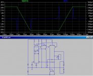
I’ve just been optimising the frequency compensation of a preliminary design of mine in which I used the frequency compensation method that Bob Cordell used in his MOSFET power amp. Namely the unity loop gain frequency is set as desired with a “Miller” feedback capacitor from the VAS collector to the inverting input, while this loop, which can be referred to as the Miller loop, is compensated with an R-C loading the LTP.
With my amplifier adequately compensated with a unity loop gain of 950kHz the slew rate was near 150V/us and operation was other wise fine, with the exception of the clipping performance.
A diode clamp is used on the VAS collector, but coming out of clipping there was significant rail sticking that could not be attributed to either the output stage or the VAS.
The cause of the sticking was tracked down to the LTP R-C. The problem here is that when the amplifier has clipped, the LTP has become overdriven and the compensation capacitor at its output attains a charge that must be gotten rid of when the amplifier comes out of clipping. This takes an amount of time, during which the amplifier’s output “sticks”.
I’ve attached a screen shot of a simplified simulation (I have omitted the cascodes and used an ideal output stage) of Bob’s amplifier to show the sticking effect, clipping at 20kHz.
The VAS is diode clamped at +/-30V. The blue trace is the current through the LTP R-C. The alternate changing and discharging of the compensation capacitance during the sticking period as the amplifier enters and leaves clipping can be clearly seen.
For the LTP R-C, Bobs amplifier used 100 ohms in series with 150pF. I am using a BJT’s for the LTP (instead of JFETs) which have higher gm. For adequate compensation of the miller loop a lower value R and a higher value C is therefore required. The sticking was therefore proportionally worse. While it can be reduced by significantly reducing the LTP’s gm with higher emitter degeneration and lightening the miller loop compensation accordingly, this is not desirable.
I’m now rethinking the compensation scheme for this amplifier. Any ideas on an alternative way to compensate the miller loop that does not cause rail sticking?
Cheers,
Glen
Attachments
- Home
- Amplifiers
- Solid State
- Bob Cordell Interview: Negative Feedback