The vias stitch two identical copper planes to form an effectively lower impedance path for high current traces or ground planes. They are also used to improve thermal conduction as the case in the snubber boards where they clamp the MOSFET body to the heatsink.
A low power 20W can be done with two 20V rails; a bit of work at the simulator and I will have it up in a couple of days......
Hugh
+1, and many thanks. Francois
Hi Folks,
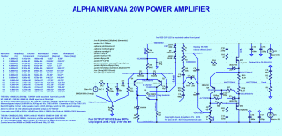
Here is the redesign of the ALPHA Nirvana for 20W//8R.
This amp uses 20V rails, and performance is not as good as the 27V rails and about half the power. But it's essentially the same amplifier with very similar harmonic profile. Interestingly at 20KHz and 12.5W//8R the H2 is at -45dB, which is almost identical to a tube like 6SL7 operating at B+ of 340V and 1.6mA plate current. It clips at just under 21W, and quiescent is 1.32A. Front end is slightly changed; R4 could be a 2k pot to set offset. Quiescent is set by the two 0.27R resistors in the sources of the outputs, which each dissipate an easy 25.5W. This output stage is ideal for passive cooling, and total power for a stereo is 105W. With >94dB/metre/watt speakers this would be a killer amp. Max loop gain is 87dB at 510Hz.
Hugh
Attachments
Hi Folks,
Here is the redesign of the ALPHA Nirvana for 20W//8R.
Hugh
Thanks Hugh: this one is next on my list!
I hope the prospected GB PCB is compatible with this version.
Jacques
No changes to pcb over the 39W version; the only changes here are component dimensions nothing else.
HD
HD
Yes, the PCB should be the same - I think there is a swap of a blue LED w a 4.75v Zener.
This is the schematic for the PCB:

This is the schematic for the PCB:
Last edited:
Hi Folks,
Here is the redesign of the ALPHA Nirvana for 20W//8R.
This amp uses 20V rails, and performance is not as good as the 27V rails and about half the power. But it's essentially the same amplifier with very similar harmonic profile.
Hugh
Hugh, did you mean to say “NOT” in “performance is not as good as the 27V rails”. If so, could you comment on how it is not as good, other than output power?
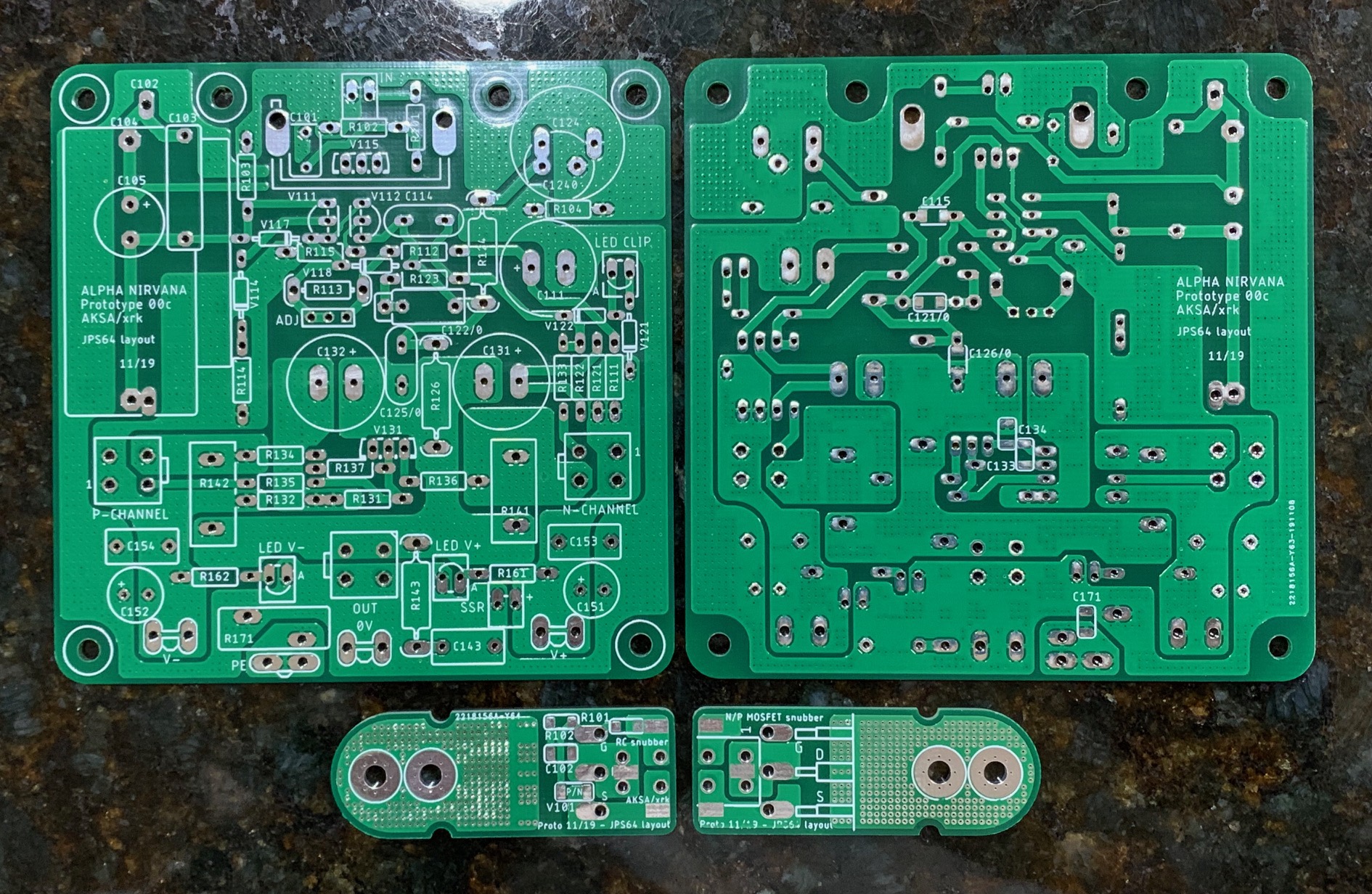
This board is going to be a joy to build. Very compact and easy parts placement. Not that many parts either. And the fiddly part of amp building: installation of MOSFETs properly aligned is a thing of the past with the quick connect flying leads. The MOSFETs are installed in a separate operation independent of the amp board.
It’s amazing how compact it is. Under 4in per edge.
It’s amazing how compact it is. Under 4in per edge.
This board is going to be a joy to build. Very compact and easy parts placement. Not that many parts either.
Hi X,
I noticed several contact points for SMD components on the main and mini boards.
While I understand the pleasure to make the circuit as small as possible I guess full TH is no longer an option for the final PCBs ?
Cheers,
Jacques
It’s amazing how compact it is. Under 4in per edge.
They almost resemble the look/shape of a ‘chipamp’ type of amplifier board.
I like how the helper pcb’s turned out 🙂
On the main board the SMT are optional mostly MLCC NP0/C0G caps with silver mica being the through hole equivalent. There are a few that are for snubbers and they are just better when compact. JPS64 will take that into consideration for the final layout. The helper (snubber) PCBs have to be SMT in order to keep the components as close to the legs as possible as they are there to stop oscillation. They are relatively large and easy to solder.
Last edited:
Thanks for the update Hugh and X. For the 2 circuits as shown, one by Hugh and the other by X, there are some transistor differences. Hugh shows type 2N5401 for Q1, Q2 and Q4, whereas on X's schematic he has these as KSA992. Also Hugh shows 2SC3503 for Q3 and on X's it is a TTC004.
The question is - what are the preferred types for this amp design. Maybe both Hugh and X can give us their views? I think it would be fair to say that Hugh's types are older and the ones X shows are more modern and would be more easy to source (but I have all of them - so what to choose?)
Regards,
Gary..
You will be ok with either schematic. Hugh’s selection is based more on fact that he has those models handy. I have run the sim with the KSA992, KSC3503, and we may even use BD140 or TTC004A for the Q4. The PCB pinouts will follow the schematic by JPS64.
Francois G,
Good question. I found after many sims that the loop gain of the 27V rail was 101dB, peaking at 250Hz. For the 20V rail it was 87dB, at 510Hz. In fb amps, any reduction of the intrinsic distortion (the distortion inherent in the topology before any fb), is largely driven by the loop gain, so with a reduction of 14dB for the smaller amp (0.0450% at +20dB) you could reasonably expect distortion around five times more than the larger amp (0.0170% at +20dB).
This is not prescriptive, because other issues intervene, such as component choices, how they behave at lower voltages and to what extent the parasitics influence the dynamic conditions. In this case, we have an improvement of almost 0.03% with the higher power amp, and it is significant that +20dB output for a 20W amp is closer to the rails than for a 39W amp. The best linearity is generally at an output around a third the peak power.
Gary S,
My original schematic is the base document, on which I have done all the careful LTSpice measurements. JPS, the layout designer, and X, the coord/production manager, have readjusted it a little for the production schematic which is identically topologically. All the LTP and VAS devices used, 5401 v. A992 and C1845 v. C3503 and outputs FQA40N25/FQA36P15 v. IRFP240/IRFP9240, will all work just fine. I like to use the 5401 because it is a very tough transistor (600mA/160V v. 50mA/120V) and its 630mW max dissipation makes it difficult to blow up, and it's a bit faster than the A992 (min 100MHz v. min 50MHz). The 5401 does have a lower beta, but it's much more linear than the very high beta A992, being flat as a billiard table from at 0.1mA to 10mA, and it's very quiet with low Cob (6pF). The problem is that the pinouts are different between 5401 and A992, and since X and JP prefer the A992 the layout is revised. The KSC3503 is an outstanding transistor for higher power amps, but the A992 is ideal for the VAS of a low power Class A. I have no difficulty with using any of these devices, but as for every component in any build, you MUST TAKE CARE WITH PINOUTS.
Ciao,
Hugh
Last edited:
Good question. I found after many sims that the loop gain of the 27V rail was 101dB, peaking at 250Hz. For the 20V rail it was 87dB, at 510Hz. In fb amps, any reduction of the intrinsic distortion (the distortion inherent in the topology before any fb), is largely driven by the loop gain, so with a reduction of 14dB for the smaller amp (0.0450% at +20dB) you could reasonably expect distortion around five times more than the larger amp (0.0170% at +20dB).
Thanks for this great explanation of the differences in expected performance. It will be instructive to see how they behave in physical builds. Thanks again.
Thanks Hugh for the detailed response to the transistor differences, and in particular the pin out warning, appreciated.
I think many will be interested.
In Audiocircle forum I wrote:
-> Power resistors for amplifier testing – the solution – Clockworks Signal Processing
In Audiocircle forum I wrote:
Archimago's Musings: The "Measurement Of Amplifiers Rig" (MOAR): Standard Tests, Loopback results, and the AMOAR Score.xrk971 detected and measured what happened with a resistance from the new DIY class A ALPHA. He put a thin metal resistor and the harmonic profile changed to H3 predominant. It changed to a carbon and was H2 predominant again. Then changed to a thick metal and kept H2 predominant.
-> Power resistors for amplifier testing – the solution – Clockworks Signal Processing
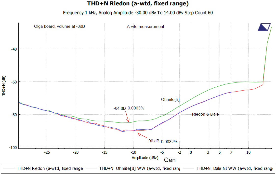
With respect to inductance, here’s the measured values:
- Dale RH 50W 4 ohm resistors are 190 nH
- Four Reidon 2 ohm 200W in series (8 ohms total) + 4′ of wire 574 nH
- Memcor 450W 4 ohm wirewound 11 uH
- Ohmite 300W 8 ohm wirewound 24 uH
Thank you, Mary. Without knowing it, I was also going to build a low inductance power resistor as a dummy load using a similar approach with heatsink and fan and thin film resistors.
This is from the article you linked:
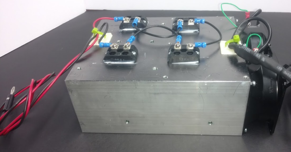
I was going to use two 300w 10ohm EBG film resistors in parallel for a 5ohm load.
EBG Resistors, manufacturer of high voltage, power thick film resistors
This is from the article you linked:
I was going to use two 300w 10ohm EBG film resistors in parallel for a 5ohm load.
EBG Resistors, manufacturer of high voltage, power thick film resistors
Last edited:
- Home
- Amplifiers
- Solid State
- Alpha Nirvana 39w 8ohm Class A Amp