Time for some power dissipation data
Running at 50MHz clock, full volume (20Vpp differential output).
5V bus:
- Digital buffers and Si570 clock, 80mA
- ES9038PRO chip in mono mode, 340mA
+/-15V for IV
- 2xOPA1622 dual I/V plus 2xOPA1612 summing amp, +/-75mA
Total power dissipation is 0.4W + 1.7W + 2.2W = 4.3W Adding the other ES9038 channel will add 1.7W + 2.2W (clock and digital buffers are common), a total of 8.2W. That's huge, but it could be argued there's little reason to run the output @20Vpp differential. At a reasonable output of a few volts, the power will be under 5W for both channels. Anyway, the decision to re-run the board with cooling copper pours was very good.
At full 100MHz and full 20Vpp output, the power will approach 10W, amazing.
OMG, yes, that sounds awfully familiar ... I wouldnt beat yourself up about it. you arent the only one that has been caught by it.Funny, I made the same mistake in the current board, the information about selecting the I2C address by using the ADDR pin is buried in the DS, the table only says at pin 41 "Chip Address select". Making that "Chip I2C Address select" would be too much to ask from ESS, of course. So I ended grounding both pin 41's (under the chip), which is obviously wrong. This is the only bug that I had to fix in the new board.
...... The strange thing is that
..... The even weirder thing is:
(????)
.....WTF? so please allow me venting for the time being... I'll eventually figure it out.
Of course
Aaand it took me 5 more minutes to figure it out. Register numbers in the DS are in decimal, not in hex as I was assuming all along. It did not make a difference for register addresses under 0x15 (which I was toying with)...
What a clusterfuck, but all is fine for now.
Yayyy!! indeed, this was an ongoing saga and I got caught up in it too. I wasnt involved in programming or building any of the logic/control stuff, I was just a builder and didnt have access to the DS at the beginning, so my apologies I couldnt be more specific and warn you about that gotcha. You would think they would make a big deal about highlighting this in subsequent datasheets ... for it to be at all ambiguous after this many revisions of hardware and software and documentation is absurd. You would think they enjoy it and leave these 'easter eggs' as rights of passage ...
Well, at least if I ever think about using an ESS chip in a design you're sharing the datasheet pain points 🙂.
Lol, you cruel, cruel man 😛 you're not wrong though.
Time for some power dissipation data
Running at 50MHz clock, full volume (20Vpp differential output).
5V bus:
- Digital buffers and Si570 clock, 80mA
- ES9038PRO chip in mono mode, 340mA
+/-15V for IV
- 2xOPA1622 dual I/V plus 2xOPA1612 summing amp, +/-75mA
Total power dissipation is 0.4W + 1.7W + 2.2W = 4.3W Adding the other ES9038 channel will add 1.7W + 2.2W (clock and digital buffers are common), a total of 8.2W. That's huge, but it could be argued there's little reason to run the output @20Vpp differential. At a reasonable output of a few volts, the power will be under 5W for both channels. Anyway, the decision to re-run the board with cooling copper pours was very good.
At full 100MHz and full 20Vpp output, the power will approach 10W, amazing.
Well, i'm not sure if the famous ESS IMD hump is still present on the 9038PRO? but with your 20Vpp, your resistor/filter values should be more ideal loading. IIRC that was one of the fixes, keeping the first stage gain higher and then reducing the output in the second stage, vs lowering the IV resistor.
Well, i'm not sure if the famous ESS IMD hump is still present on the 9038PRO?
Hump is mostly depend of a I/V and summing amp.
Well, here's another example about how much we can trust reports from various sources. And that nothing can replace your own measurements (if you can do them).
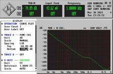
In despite of multiple reports that the THD/IMD hump in the ESS DACs exists only in the low(er) end DACs (ES9038QM2) and the ES9038PRO is unaffected (including on ASR, ESS THD ‘Hump’ Investigation | Page 6 | Audio Science Review (ASR) Forum and the following), this is not true. The ES9038PRO has the hump as big and fat as the other ESS DACs, see attached, this is THD, IMD is the same only, scaled higher.
X axis is in dBFS.
Now, let's see if the same method of hump elimination works for the PRO chip, I would think it will. Do I need to say again "**** ESS"?
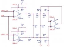
P.S. Simplified schematic (decouplings, etc... removed) for half the current IV stage is also attached.
In despite of multiple reports that the THD/IMD hump in the ESS DACs exists only in the low(er) end DACs (ES9038QM2) and the ES9038PRO is unaffected (including on ASR, ESS THD ‘Hump’ Investigation | Page 6 | Audio Science Review (ASR) Forum and the following), this is not true. The ES9038PRO has the hump as big and fat as the other ESS DACs, see attached, this is THD, IMD is the same only, scaled higher.
X axis is in dBFS.
Now, let's see if the same method of hump elimination works for the PRO chip, I would think it will. Do I need to say again "**** ESS"?
P.S. Simplified schematic (decouplings, etc... removed) for half the current IV stage is also attached.
Attachments

Last edited:
The hump may be an artifact or interaction with the following analog stages, but I wonder why we don’t see this with AK4499.
I was curious to see if you would experience it with OPA1622 as I/V converter. I understand your rationale for choosing it here but it’s a bit slow to deal with some of the trash that comes out of the DAC linearly perhaps.
I was curious to see if you would experience it with OPA1622 as I/V converter. I understand your rationale for choosing it here but it’s a bit slow to deal with some of the trash that comes out of the DAC linearly perhaps.
Last edited:
The hump seems like a result of noise out of the dac modulator on the analog outputs driving the opamps into some nonlinearity. Maybe RF demodulation in the input stages, or else slewing elsewhere. Adjusting component values may ease the strain on the opamps a little and allow them back into linearity. Just my two cents 🙂
Last edited:
Just my two cents 🙂
Worth exactly two cents, your guess is as good as anybody else's. You forgot to add something about "noise floor modulation" and "close-in phase noise".
Did a bit of surgery on the board and replaced the OPA1622 with an OPA1612 (which is a dual OPA1611) in dead bug position, also tried an OPA1642 and then an OPA1656 (I guess I now qualify as an "op amp roller"). These are much faster (3x) than the OPA1622. Absolutely no change in the THD hump with any of these. The hump has nothing to do with the op amp(s).
Also doesn't depend on the input signal frequency, clock frequency (from 100MHz to 12.5MHz) or sampling frequency (from 48KHz to 384KHz).
Also doesn't depend on the input signal frequency, clock frequency (from 100MHz to 12.5MHz) or sampling frequency (from 48KHz to 384KHz).
Last edited:
Did a bit of surgery on the board and replaced the OPA1622 with an OPA1612 (which is a dual OPA1611) in dead bug position, also tried an OPA1642 and then an OPA1656 (I guess I now qualify as an "op amp roller"). These are much faster (3x) than the OPA1622. Absolutely no change in the THD hump with any of these. The hump has nothing to do with the op amp(s).
Also doesn't depend on the input signal frequency, clock frequency (from 100MHz to 12.5MHz) or sampling frequency (from 48KHz to 384KHz).
I think your problem could be board layout.
The board layout looks beautiful... from an aesthetic POV but that doesn't mean it is optimal from an electronic POV.
TCD
I think your problem could be board layout.
The board layout looks beautiful... from an aesthetic POV but that doesn't mean it is optimal from an electronic POV.
I don't think so. In fact, somebody on ASR pointed me to a bunch of ES9038PRO commercial products that do have the hump.
It is what it is, will try the counter-hump (I would not bet a dime that any solution doesn't come without some trade-offs), otherwise CS43198 is probably my next best bet. AK4499 is for 2022 (if that).
BTW, the Si570 with its high low frequency phase noise and horrible close in phase noise is perfect, can't get any better in a DAC, measurement wise. Too bad some can hear it's horrible screechy sound
 .
.
Last edited:
Nah, I don't think it's layout driven, as it looks consistent with all other examples in shape, so if it's layout related, it's consistent among them all, which seems unlikely.
I'm betting it's in the geometry of the dac output. Have you tried inverting the phase and maybe playing with the internal rputing and summing, then seeing if the shape remains the same?
Yes, that cheap crystal semi dac is quite the surprise, isn't it? Honestly these distortions are so far down it's pretty academic. Matters more for you since it's an instrument, but even then it's really not much to worry about.
Yes, that cheap crystal semi dac is quite the surprise, isn't it? Honestly these distortions are so far down it's pretty academic. Matters more for you since it's an instrument, but even then it's really not much to worry about.
It would be a real winner for measurement use if they made a version that consumed a bit more power but had better filter performance at 192 kHz and above, or at least accepted 8x rates from an external filter. That and pushed the out-of-band noise out a bit farther.
- Home
- Design & Build
- Equipment & Tools
- ADCs and DACs for audio instrumentation applications