No idea, sometimes vendors give you 8-bit addresses with the R/W bit added because they think their customers are idiots.
What Chris said above. That's caused me no end of confusion in the past.
I'm surprised by the power consumption of the DAC chip, that seems excessive to say the least. 4 watts per ES9038PRO? The datasheet suggests just over a watt from a 5V rail for 'note 1' conditions? Ie 222mA consumption.
I'm surprised by the power consumption of the DAC chip, that seems excessive to say the least. 4 watts per ES9038PRO? The datasheet suggests just over a watt from a 5V rail for 'note 1' conditions? Ie 222mA consumption.
Its not uncommon for some I2C libraries to use the 8-bit addressing paradigm. In that view each device has two addresses, one for writing, the other for reading (which is always the write address plus 1). Its not so hard to think of it in that way.
It is not 4W for the chip, this is the total power for one channel. 2.5W is the ES chip + regulators + digital buffers + Si570 oscillator, the rest is for the balanced I/V stages ( 2 x OPA1622 duals plus 2 x OPA1611). And this is @100MHz, the data sheet specifies the currents intake @40MHz. There are blurbs on the Internet that @100MHz the current intake increases significantly, hence my #464 question about.
The I2C 0x90 data sheet address doesn't make any sense, if bit 7 R/W is ignored, the rest is 0x10 which is not the real ES chip address (0x48). 0x48 is 0x90 shifted right by 1 bit, absurd. Most likely yet another bug in the documentation, who knows how many more are out there...
The I2C 0x90 data sheet address doesn't make any sense, if bit 7 R/W is ignored, the rest is 0x10 which is not the real ES chip address (0x48). 0x48 is 0x90 shifted right by 1 bit, absurd. Most likely yet another bug in the documentation, who knows how many more are out there...
There is always mistakes in the ESS datasheets, particularly when it comes to this area (I2C addressing) strange, because they are particularly heavy in that area vs analogue application information. I have known several designers who did a first spin before finding errors in the DS caused them to do a respin and I believe one even had a first run assembled (thankfully a short run). Coincidentally (maybe not) this was an error that interfered with the chip address in a dual mono 9018pro dac and it could not be fixed with a patch, as the pin was grounded under the chip. I wonder if this is an error that persists from the 9018 DS ...
Indeed, i'm finicky about routing too and do most manually, since I do a lot of polygon/plane routing and while I believe altium will use this if you ask in autoroute mode, diptrace does not. I superstitiously try to avoid right angle routing when I can, as least for high current, or high speed traces. something about the electrons flying off the board around corners ... 🙂 Autorouting results seems all about setting up the rules and net-classes well. I generally avoid it, but I have been getting better at it. definitely never just hit autoroute, but I have started on occasion clearly defining netclasses and selecting only a patch of less critical components and autoroute those alone and cycle through versions until I get one that I can work with and edit that til i'm 'happy'.
Indeed, i'm finicky about routing too and do most manually, since I do a lot of polygon/plane routing and while I believe altium will use this if you ask in autoroute mode, diptrace does not. I superstitiously try to avoid right angle routing when I can, as least for high current, or high speed traces. something about the electrons flying off the board around corners ... 🙂 Autorouting results seems all about setting up the rules and net-classes well. I generally avoid it, but I have been getting better at it. definitely never just hit autoroute, but I have started on occasion clearly defining netclasses and selecting only a patch of less critical components and autoroute those alone and cycle through versions until I get one that I can work with and edit that til i'm 'happy'.
Last edited:
the power consumption is over the top, but as they seem to increase the performance of each revision of their SOTA part by parallelling more dacs in each successive part, it unsurprisingly results in higher current demands and lower output impedance. 9018pro was ~32mA at ~95Ω IIRC in mono mode, word on the street was they doubled the number of dacs in the 9028 and added a few other features so that gives us around 64mA, so perhaps they've doubled it again?
Last edited:
Bit 0 is the R/W bit, the rightmost bit.
From one I2C library:
"i2c_start(addr)
Initiates a transfer to the slave device with the 8-bit I2C address addr. Note that this library uses the 8-bit addressing scheme different from the 7-bit scheme in the Wire library. In addition the least significant bit of addr must be specified as I2C_WRITE (=0) or I2C_READ (=1). Returns true if the addressed device replies with an ACK. Otherwise false is returned."
GitHub - felias-fogg/SoftI2CMaster: Software I2C Arduino library
Last edited:
The I2C 0x90 data sheet address doesn't make any sense, if bit 7 R/W is ignored, the rest is 0x10 which is not the real ES chip address (0x48). 0x48 is 0x90 shifted right by 1 bit, absurd. Most likely yet another bug in the documentation, who knows how many more are out there...
I think you got this part wrong. The direction bit to ignore is bit 0.
Otherwise you are correct about the quality of ESS datasheets.
Yeah, sorry, brain fart here. Bit 0 is indeed the R/W so 0x90 is in fact 0x48 with a 0 appended at the right, 0x48 = 1001000 0x90 = 1001 0000. Makes some sense now, although this way of specifying the I2C address is still BS in my book. When I read "address" I expect the address not some weird construction than includes an extra unrelated (to the address) bit.
Ref. power consumption, I just tested, at XIN/8 (12.5MHz) the current intake on +5V drops at 228mA (from 480mA @100MHz). At XIN/2 (50MHz, close to the DS specification) current intake is 340mA. Subtract the some 80mA used by the digital buffers and the Si570 and get 260mA for the ES chip (all voltages) which is reasonably aligned with the data sheet (220mA @40MHz).
Ref. power consumption, I just tested, at XIN/8 (12.5MHz) the current intake on +5V drops at 228mA (from 480mA @100MHz). At XIN/2 (50MHz, close to the DS specification) current intake is 340mA. Subtract the some 80mA used by the digital buffers and the Si570 and get 260mA for the ES chip (all voltages) which is reasonably aligned with the data sheet (220mA @40MHz).
ah, sorry, to be clear, I had my own brain flatulence, I was just talking about power consumption in the AVCC area, not total for the DAC. Sorry for the confusion. So doubling the number of dacs placed in parallel on the die each revision, which would scale the current consumption for that area more so than the control and digital, which would/should remain roughly the same (for a given FS).
Last edited:
Good to hear you are on top of it. It would be boring if they just did something in line with every other manufacturer though, wouldnt it? ... eh... eh?
I'm pretty sure that the person who wrote AK4137 datasheet came from ESS (or after writing that datasheet left AKM to write datasheets for ESS) 😀
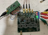
Looking good!! So no more issues with the terminally depressed power supply? all related to the larger than expected power draw? My apologies if you explained earlier and I missed it.
I have known several designers who did a first spin before finding errors in the DS caused them to do a respin and I believe one even had a first run assembled (thankfully a short run). Coincidentally (maybe not) this was an error that interfered with the chip address in a dual mono 9018pro dac and it could not be fixed with a patch, as the pin was grounded under the chip. I wonder if this is an error that persists from the 9018 DS ...
Funny, I made the same mistake in the current board, the information about selecting the I2C address by using the ADDR pin is buried in the DS, the table only says at pin 41 "Chip Address select". Making that "Chip I2C Address select" would be too much to ask from ESS, of course. So I ended grounding both pin 41's (under the chip), which is obviously wrong. This is the only bug that I had to fix in the new board.
This is going to be a gigantic mess... I cannot write to regs 38-41 what I would like to (or reading is wrong). I am writing to all registers 38-41 the same (use Input 3 for both L/R, this is mono mode, stereo mode is disabled, autoconfig for inputs is disabled)
write_to(reg, b'\x33')
and get back when reading the registers:
Reg 0x38: bytearray(b'3')
Reg 0x39: bytearray(b'3')
Reg 0x40: bytearray(b'\xa8')
Reg 0x41: bytearray(b'\x01')
Which is completely bollocks. However, the output is fine! Aaarrgghh... must take a break, this is too frustrating.
write_to(reg, b'\x33')
and get back when reading the registers:
Reg 0x38: bytearray(b'3')
Reg 0x39: bytearray(b'3')
Reg 0x40: bytearray(b'\xa8')
Reg 0x41: bytearray(b'\x01')
Which is completely bollocks. However, the output is fine! Aaarrgghh... must take a break, this is too frustrating.
Expired before editing. The strange thing is that registers 37 and 38 (and all the other registers I am R/W-ing) are taking the 0x33 value (0x33=b'3') however 40 and 41 do not. They have the values:
Reg 40: 0xA8
Reg 41: 0x01
and after overwriting with 0x33 they come up with exactly the same values, like the write never happened. These values don't make any sense according to the DS, they are supposed to be 0x54 and 0x76 by default, wtf?
The even weirder thing is:
- 0xA8 that I'm reading from 0x40 is the default 0x54 value (according to the DS), circular shifted left 1 bit
- 0x01 that I'm reading from 0x41 is the default 0x76 value (according to the DS), circular shifted left 1 bit, and complemented (????)
So again, WTF? And why can't I write new values? I understand fighting the beast is part of the game, so please allow me venting for the time being... I'll eventually figure it out.
Aaand it took me 5 more minutes to figure it out. Register numbers in the DS are in decimal, not in hex as I was assuming all along. It did not make a difference for register addresses under 0x15 (which I was toying with)...
What a clusterfuck, but all is fine for now.
What a clusterfuck, but all is fine for now.
- Home
- Design & Build
- Equipment & Tools
- ADCs and DACs for audio instrumentation applications