No problem. It was never specified in the 9018pro and given the pin descriptions, I had always powered them separately, so, while it makes you wonder, i'm not arguing with a $50-70 reduction in my BOM
also, just a reminder @ syn08, running high FS and mono, your 1.2V pins should be increased to 1.3V
also, just a reminder @ syn08, running high FS and mono, your 1.2V pins should be increased to 1.3V
Last edited:
yes, its not well worded at all, if you dont catch the notes section near the bottom of page 5, you would think they are separate.
Thanks, I didn't catch the p. 5 foot note and, as a result, in the layout above I included separate power supplies for digital 1.2V. Once I get the boards tomorrow, I have to avoid populating those extra power supplies, otherwise they will collide with the 1.2V analog supplies (if the pins are internally connected). Yes, I am aware of the 1.3V requirement for running @100MHz, thank you.
**** ESS, their NA distributor once again rejected my order for ES98x2PRO ADC chips and the application for the data sheet, once again because I don't have a company behind (and yes, I tried mocking something, didn't work, they checked, asked for more proof, website, previous products, etc...). This is beyond ridiculous.
Last edited:
It's sadly not the worst out there. Try dealing with Broadcom, Qualcomm, or Marvell for example. Even if you are a decent size company, if they don't smell 100k-1M+ qty they don't really care to communicate. If you want one of the parts available at Digi-Key, fine, but any of the NDA protected parts or SoCs, good luck.
Well, I am dealing with the suspects you quoted on a weekly basis, and while you are correct in your assessment it is also true that for these companies high volumes/low prices is part of their business model.
ESS doesn't match this type of business model by any metric. Minuscule market and high prices (with huge margins, I presume).
ESS doesn't match this type of business model by any metric. Minuscule market and high prices (with huge margins, I presume).
Given the costs of startup for an lsi chip profits don't exist until you hit 1 million units.
ESS has always been difficult. CSR was good until Qualcom bought them and then support was only for tier 1 customers. The rest get second rate support through distributors. It makes some sense if you are pushing the envelope of what can be done to only support big guys but then only yesterday's projects get done. Little really inventive happens inside the constraints of the big tier 1 companies.
ESS has always been difficult. CSR was good until Qualcom bought them and then support was only for tier 1 customers. The rest get second rate support through distributors. It makes some sense if you are pushing the envelope of what can be done to only support big guys but then only yesterday's projects get done. Little really inventive happens inside the constraints of the big tier 1 companies.
The issue I run into is that we’re sometimes working on low volume but extremely expensive capital equipment. We don’t care if they want to charge us a lot, but if we need something, we need something. That means we sometimes run into issues when we need something from one of the big vendors and it’s not one of the parts that’s stocked at normal distributors. TI, AD, Maxim are great, but some are not.
I started to avoid&hate Maxim since they began obsoleting parts without any respect for existing customers. Any decent chip manufacturer creates its own wafer bank before they decide announcing the obsolescence of a product, with a buffer of at least few years for last time purchase and then maintenance/support parts. Not Maxim, in 3 months the obsolete product was gone, without any replacement or second source, effectively screwing their customer base. Apparently they got better in the last decade or so.
I can tell, Broadcom has absolutely no price/performance competitors for telecom CPE (Customer Premises Equipment) SoC's. This is entirely based on high volumes and penny pinching in support. You have to be an 1M+/year customer to get any kind of attention from their FAEs and SDK teams. Without that, you found a bug in the SDK, tough ****, you live with it and work around, if you can. If you can't, they won't shed a tear over your business.
I can tell, Broadcom has absolutely no price/performance competitors for telecom CPE (Customer Premises Equipment) SoC's. This is entirely based on high volumes and penny pinching in support. You have to be an 1M+/year customer to get any kind of attention from their FAEs and SDK teams. Without that, you found a bug in the SDK, tough ****, you live with it and work around, if you can. If you can't, they won't shed a tear over your business.
Last edited:
Given the costs of startup for an lsi chip profits don't exist until you hit 1 million units.
That's not entirely true, there are more factors involved here.
It is certainly true for the products built in the bleeding edge processes, like memories. To have a ballpark, an EUV (Extreme UV) lithography scanner doing 80 wafers/hour in a typical 5-7nm node memory process costs north of 120M$, and there are at least 10 masks that require that resolution, then at least 15-20 machines are required for the sweet spot between output and cost. That's why very few companies have their own fabs today, most (including Broadcom, ESS, Qualcomm, Marvel, etc...) are using foundry services, like TSMC.
You have to be an 1M+/year customer to get any kind of attention from their FAEs and SDK teams.
1M+/year doesn't get you as much attention as you might think. At least the kind of attention that one might find useful.
Trust me, I got all the attention I need, at least from Broadcom, Marvel and a few others in the same class 😀.
1M+/year doesn't get you as much attention as you might think. At least the kind of attention that one might find useful.
Depends what you're buying. Five cent regulators, probably not. Four digit USD FPGAs, you'll get some pretty nice treatment.
That's not been my/our experience. Although not in their stated top 5 customer list, we do routinely get cited as one of their top dozen or so. By them.Trust me, I got all the attention I need, at least from Broadcom, Marvel and a few others in the same class 😀.
They are right there when they're trying to sell something, but try to get details or help when you discover a bug or something that doesn't match the manual...
But, if it's working for you, great! Be happy, then.
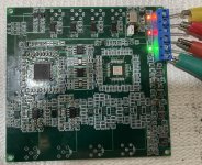
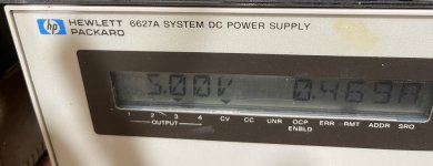
DAC is coming up, one half (one channel) only, for testing purposes. OMG, this monster is power hungry... @100MHz clock sucks half an amp from the 5V supply (post regulated to 3.3V and 1.2V). And this is with idle outputs, nu current drawn in the I/V. Measured the peak current at the I/V (+/-15V) by cutting the clock, is 170mA meaning 120mAeff. I'm afraid I underestimated the power dissipation... it's 5W for the 5V plus 3.5W from +/-15V total of 8.5W for both channels. That's a power amplifier, not a DAC...
Attachments
Last edited:
That's a lot of power for just a DAC for sure.
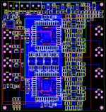
Always interesting to see personal routing styles. I see you are a fan of the 90 degree bend 🙂.
Always interesting to see personal routing styles. I see you are a fan of the 90 degree bend 🙂.
Well, it’s actually two DACs, but still a lot of power, 4W per DAC (including the regulators).
Never thought about 90 degrees traces, it was the most natural (to me) style. I never use autoroute, the result was always a disaster (or I don’t know how to use the tool), everything is 100% manual routing. I use 45 degrees only when forced by spacing.
Already revised the board, to include a top layer ground copper pour (to help with cooling) and a few other minor changes.
For now, starting testing, using a FT2232H USB/I2C adapter, and the pyftdi library, to program the ESS9038 registers and the Si570 clock.
Yeah, still lot of power. I guess ESS has the Q2M versions for those that care about that sort of thing. That's about what my dual LTC2387 board uses, but it has an FPGA, 1 GB of DDR3, and 6 ADN465x LVDS isolators...
Ah, makes sense now on the traces. Do you use Cadence or KiCad? I'd guess it's not Altium since you have to manually change to get 90 degree corners. Not that it matters.
Ah, makes sense now on the traces. Do you use Cadence or KiCad? I'd guess it's not Altium since you have to manually change to get 90 degree corners. Not that it matters.
New board layout sent to fab, with extra top layer copper pour (ground connected) to help with cooling. Small fixes and changes (removed the 1.2V digital power supplies, separated the Si570 power supply from the ES9038PRO oscillator power supply, added small circuit to the LTC2924, to signal the end of power sequencing cycle), general layout cleanup. Hopefully it's the last iteration, price for 10 pcs. 4 layers boards is cheaper than the DHL shipping to Canada, but the total 10 days to wait until delivery is in general booooring. Not in this particular case, I need to do the measurements and start the software dev.
Attachments
I am amazed by the amount of confusion in the ES9038PRO data sheet, here’s the latest one:
The DS states that the I2C address of the ES9038 chip with the ADDR pin grounded is 0x90... how come??? The I2C bus spec says only 128 devices (in fact, there are even less) are allowed on the I2C bus, since bit 7 is the R/W bit. Doing a bus scan using a FTDI2232H board shows that the actual address of the ES9038PRO chip is actually 0x48. Looking at the bits, 0x48 is exactly 0x90 shifted right by 1 bit.
Am I missing here something, or ESS went completely nuts? The Si570 device specified at address 0x55 is exactly where it is supposed to be on the I2C bus.
- Home
- Design & Build
- Equipment & Tools
- ADCs and DACs for audio instrumentation applications