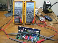
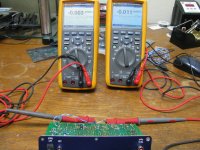
agdr - Okay, I have taken some measurements of voltage rails and the points that you marked. Tomorrow I hook voltage rails to scope.
Based on these, tomorrow I can do more scope work if want.
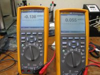
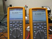
The mark on the left side of the chips to the ground gives -7mV shortly after the relay has kicked in, it starts to go down to -3mV as the amp works for few minutes with small oscillations.
Right side is -0.6mV with small oscillations, pretty stable.
Voltage rails:
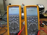
Positive rail shows 30mV AC with small oscillation.
Negative rail shows 25mVAC with small oscillation.(It shows around 100mV when I hook up the voltmeter probes and it quickly goes down to around 25mV AC and settles).
All the measruments are done with left resistors (1Ohm) still unsoldered.
I have also found a very neat way to unsolder those chips(I make a big blob of solder to connect all fins and the chip just falls out 🙂, quite satisfying!)
Based on these, tomorrow I can do more scope work if want.
The mark on the left side of the chips to the ground gives -7mV shortly after the relay has kicked in, it starts to go down to -3mV as the amp works for few minutes with small oscillations.
Right side is -0.6mV with small oscillations, pretty stable.
Voltage rails:
Positive rail shows 30mV AC with small oscillation.
Negative rail shows 25mVAC with small oscillation.(It shows around 100mV when I hook up the voltmeter probes and it quickly goes down to around 25mV AC and settles).
All the measruments are done with left resistors (1Ohm) still unsoldered.
I have also found a very neat way to unsolder those chips(I make a big blob of solder to connect all fins and the chip just falls out 🙂, quite satisfying!)
agdr - Okay, I have taken some measurements of voltage rails and the points that you marked.
Very good! OK I'm convinced the output chips are bad. They are wired up as unity voltage gain, so the output should never be more than the input, but especially not 100mV! Maybe it was a bad batch of chips or some power supply issue. I'll send you new, matched, chips. 🙂
Very interesting about your technique on getting the SIP chips out! So you just run a bead of solder along all 8 pins and it comes out! Good to know! I do something similar with the voltage regulators in the O2 headphone amp. The 3 pins are in a row (TO-220 case) and the PCB holes are pretty big. I just put a piece of solder wick across the 3 pins, heat it, and the part drops right on the floor. 🙂 I've never used "chip quick" but sounds like it works like this too. Stays hot enough for a few seconds to be liquid, enough to heat up several pins at once.
I'll send you another PM with some information.
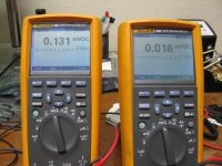
Funny that only left side is affected.
I have looks datasheet of voltage regulators and it says that output noise is around 60 μV RMS which seems quite optimistic.
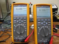
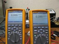
Voltmeter measures around 25mV on both rails when everything is turned on, is that okay?
I should be able to look it up on scope soon enough.
I have looks datasheet of voltage regulators and it says that output noise is around 60 μV RMS which seems quite optimistic.
Voltmeter measures around 25mV on both rails when everything is turned on, is that okay?
I should be able to look it up on scope soon enough.
Funny that only left side is affected.
I have looks datasheet of voltage regulators and it says that output noise is around 60 μV RMS which seems quite optimistic.
Voltmeter measures around 25mV on both rails when everything is turned on, is that okay?
I should be able to look it up on scope soon enough.
25mV sounds high, especially given the pre-regulators. I'll scope an ODA here and see what the ripple measures.
It could be the 12.5Vdc component is messing with the AC reading on your meter's AC scale. Try putting a 1uf to 10uf capacitor in series with the meter lead to block the DC, watching capacitor polarity there of course. On the my Fluke 289 DMMs there is a special mode that shows both AC and DC offset component, which is actually a function on the DC scale. From the manual it seems that DC offset on the AC scale would alter the reading. A scope is definitely the best way to go, if possible! 🙂
Last edited:
A scope is definitely the best way to go, if possible! 🙂

Pretty flat 🙂
Both channels are that flat.
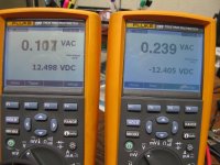
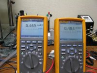
Looks good! I was able to get some measurements made today, photos below. These are on a previous-generation V2.0 board. Circuitry is the same as the V2.1, I just made some minor cosmetic changes in V2.1. The V2.0 was just one I already had opened up on the shelf. 🙂
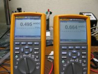
The first 3 are the power supply rails. One meter is on each rail, with the displays set to show AC ripple at the top and the DC voltage at the bottom. The positive rail is 12.50V with 120mVrms of ripple, while the negative rail is -12.40 with 240mVrms of ripple. On this board I didn't even bother getting the rails any closer than 0.1Vdc since it was a test board. 🙂 So it looks like your 25mVrms ripple is very good! This board is running 5x - 10x more.
The LT3015 datasheet shows a maximum of 25mV load regulation for the fixed 12V version of the chip at room temperature, or 62mV maximum over the whole temperature range. For the adjustable version, which is what is being used in the ODA, their spec is kind of hard to translate to other voltages. Note 2 says adjust pin tied to output pin. The ripple will probably "gain up" with the adjust pin set with resistors. But again, your readings all sound within spec for rail ripple. I just wanted to make sure there were not volts of ripple on the rails!
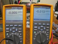
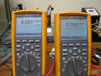
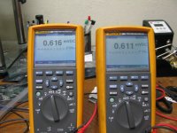
The next 3 are the output offset of the amplifer. When I first turned this ODA on, which has been sitting here for a couple of years, the offsets were +40 microvolts and + 65 microvolts. I re-adjusted the trimmers for near minimum, which gives the -3 microvolts and -11 microvolts on the two channels. But the 3rd photo is taken about 5 minutes from the first one and already the channels have thermally drifted 2 microvolts to -5uV and -13uV, which is typical of the drift to expect. These numbers are present from the moment the relay closes (about 3 seconds after turn-on), so your 100mV measurement on the amplifier output is definitely way off from normal.
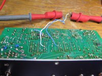
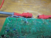
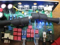
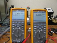
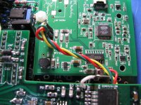
Then the final 3 are the inputs to the 3 output chips on each channel, the two points circled in the photo on post 940 above. -106 microvolts on one channel and +292 micovolts on the other, both typical of what should be there. I think you measured 7mV on one of yours, which again is way off. So it does look like you have some bad output chips.
I should be able to get your stuff in the mail tomorrow morning. 🙂
The first 3 are the power supply rails. One meter is on each rail, with the displays set to show AC ripple at the top and the DC voltage at the bottom. The positive rail is 12.50V with 120mVrms of ripple, while the negative rail is -12.40 with 240mVrms of ripple. On this board I didn't even bother getting the rails any closer than 0.1Vdc since it was a test board. 🙂 So it looks like your 25mVrms ripple is very good! This board is running 5x - 10x more.
The LT3015 datasheet shows a maximum of 25mV load regulation for the fixed 12V version of the chip at room temperature, or 62mV maximum over the whole temperature range. For the adjustable version, which is what is being used in the ODA, their spec is kind of hard to translate to other voltages. Note 2 says adjust pin tied to output pin. The ripple will probably "gain up" with the adjust pin set with resistors. But again, your readings all sound within spec for rail ripple. I just wanted to make sure there were not volts of ripple on the rails!
The next 3 are the output offset of the amplifer. When I first turned this ODA on, which has been sitting here for a couple of years, the offsets were +40 microvolts and + 65 microvolts. I re-adjusted the trimmers for near minimum, which gives the -3 microvolts and -11 microvolts on the two channels. But the 3rd photo is taken about 5 minutes from the first one and already the channels have thermally drifted 2 microvolts to -5uV and -13uV, which is typical of the drift to expect. These numbers are present from the moment the relay closes (about 3 seconds after turn-on), so your 100mV measurement on the amplifier output is definitely way off from normal.
Then the final 3 are the inputs to the 3 output chips on each channel, the two points circled in the photo on post 940 above. -106 microvolts on one channel and +292 micovolts on the other, both typical of what should be there. I think you measured 7mV on one of yours, which again is way off. So it does look like you have some bad output chips.
I should be able to get your stuff in the mail tomorrow morning. 🙂
Attachments

Last edited:
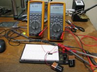
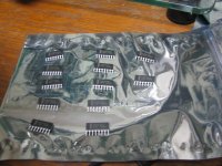
bozoc - I found a problem! 🙂 I put together a chip-test jig tonight and tested a bunch of new NJM4556A's that arrived from Mouser a couple of days ago. Well the chip offsets are not what they used to be. They used to be fairly consistently around +1.5mV. That has been the case too for many O2 headphone amplifiers I've measured over the years with 3mV output offsets. 1/2 of that is the 1.5mV of the NJM4556A buffers and the other half the input bias current multipled by the 40.2K ground return resistor that NwAvGuy used.
Well the current batch has offsets that are much smaller, and are centered around zero - both polarities - more like I would expect to find with chip offsets. I'll take a guess that NJM has tightened up their process a bit. None of this would explain the 100mV you measured, that still must be a bad chip or chips, but it would explain if you were getting something in the -1.5mV to -3mV output range and were not able to zero it out.
Very interesting! I've built up several ODAs over the years and haven't run into this. Must be a fairly recent chip change.
So I'm sending you the six NJM4556A chips with the measurements below. I picked these out of the bunch to all have positive offsets that the zeroing circuit will be able to cancel. Keep in mind the input bias currents multiplied by the 4.99K ground return resistors (R43 and R43) are also part of what the zeroing circuit is correcting.
Once you get the NJM4556A's removed please measure the voltage at the two input points above and let me know what you get (the photo in post 940).
Photos-
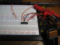
The first photo is just the test setup on a breadboard. Two 9V batteries for power, then output shorted to inverting input on each chip half and each non-inverting input shorted to ground.
The next six are your new chips. All positive offsets. 🙂
The final 3 are some of the random samples, showing the offsets can go positive and negative now. The largest offset I found in the bunch was 0.707mV. The other half of that chip was 0.211mV.
Well the current batch has offsets that are much smaller, and are centered around zero - both polarities - more like I would expect to find with chip offsets. I'll take a guess that NJM has tightened up their process a bit. None of this would explain the 100mV you measured, that still must be a bad chip or chips, but it would explain if you were getting something in the -1.5mV to -3mV output range and were not able to zero it out.
Very interesting! I've built up several ODAs over the years and haven't run into this. Must be a fairly recent chip change.
So I'm sending you the six NJM4556A chips with the measurements below. I picked these out of the bunch to all have positive offsets that the zeroing circuit will be able to cancel. Keep in mind the input bias currents multiplied by the 4.99K ground return resistors (R43 and R43) are also part of what the zeroing circuit is correcting.
Once you get the NJM4556A's removed please measure the voltage at the two input points above and let me know what you get (the photo in post 940).
Photos-
The first photo is just the test setup on a breadboard. Two 9V batteries for power, then output shorted to inverting input on each chip half and each non-inverting input shorted to ground.
The next six are your new chips. All positive offsets. 🙂
The final 3 are some of the random samples, showing the offsets can go positive and negative now. The largest offset I found in the bunch was 0.707mV. The other half of that chip was 0.211mV.
Attachments
-
 IMG_4780.JPG645.4 KB · Views: 83
 -
 IMG_4782.JPG584.2 KB · Views: 85
 -
 IMG_4781.JPG555.1 KB · Views: 84
 -
 IMG_4803.JPG528.6 KB · Views: 83
 -
 IMG_4802.JPG483.8 KB · Views: 87
 -
 IMG_4801.JPG557.4 KB · Views: 91
 -
 IMG_4795.JPG530.5 KB · Views: 93
 -
 IMG_4794.JPG514.4 KB · Views: 89
 -
 IMG_4793.JPG539.2 KB · Views: 89
 -
 IMG_4792.JPG540.2 KB · Views: 104
Last edited:
bozoc -
Whoops, I forgot something. 🙂 In the previous post I had the non-inverting inputs grounded, not going through a 4.99K ground return resistor as in the real circuit. I had forgotten how much of a difference the input bias current makes on these chips. The photos below are the same 6 chips I'm sending you as in the photos above, but now the inputs are going through a 4.99K resistor to ground. All the measurements are now in the 0.5mV to 0.8mV range, much closer to what the circuit is expecting. This test is important as it shows the direction of the input bias current is such as to cause a positive additional voltage drop across the ground return resistor. So not as many of the random sample of chips as I thought had negative input offsets, when this factor is taken into account.
In these tests just the two chip halves are going through the resistor, but in the actual circuit all 6 halves go through. So the net result should be right back in the 1.0 to 1.5mV range, as expected. I'll have to go back and re-read the previous chip tests, but I probably had the inputs going through a resistor like this. In the O2 the resistor is 40.2K vs. 4.99K here (10K pot in the O2 vs. a 1K pot here, this resistor effectively loads the pot in both amps). So the chip's input bias current has an even greater effect in the O2.
The first two photos are the test setup. The blue resistor is the 4.99K. The remaining 6 are the six new chips.
So the diagnosis is still that you wound up with some bad chips. 🙂
Attachments

Last edited:
So, if only one half of the three chip is bad. It could be messing up the whole side. The chips with the small negative offset are not suitable for ODA because of ODA's zeroing circuit.
With the last test you made(with 4.99K ground resistor), you said not as many chips produce negative offset, that is a small number of chips?
I am also wondering how different packages of the same chip behave - DIP(SIP) and SOIC?
Not connected to text above, random though - would 100% SMT ODA have any advantages besides being bit cheaper?
Hi bozoc! The small negative offsets got swamped by the offset produced with the input bias current multiplied by that 4.9K resistor. So an offset of -0.100mV with the chip input grounded might become +0.400mV when that 4.9K offset voltage is added.
Most definitely, if half a chip is bad it can mess up the whole thing since the inputs and outputs are all tied together with the chips in parallel.
Good question about DIPS vs. SIPs! I've only tested the SIPs. It would be interesting to see what the NJM4556A DIPs do. I've just been assuming it is exactly the same silicon just placed in the different packages. But that may not be the case.
When I first came up with the ODA I was considering using LME49600 buffers (surface mount) instead of the NJM4556As. But I decided not to go that way for a few reasons. One big one is I wanted the ODA to stay as faithful as possible to NwAvGuy's O2 design. Essentially a beefed up O2. Another is that OPC here already has several nice amps using the LME49600 and I wanted to come up with something new and different for the ODA. 🙂 And yet another is PCB space considerations. By using the SIP chips I could make good use of the vertical space and keep the amp compact (and the PC board cost down). The LME49600s require quite a bit of foil surface area for heat sinking. I did consider discrete transistors for the output, but that would stray from the O2's all-chip design, plus there were quite a few headphone amps out there already with discrete outputs.
A recent chip that could be used in something like an ODA is the OPA1622, but I've concluded that chip is best fed directly by a DAC. If NwAvGuy were still around maybe that would be the next big thing, a combination single-board "ODAC" + "O2" using the OPA1622 chips for the O2 part. 😀
Oleg here has a really nice OPA1622 board whipped up in another thread. Maybe he will add a DAC to that some day. 🙂
Last edited:
Oleg here has a really nice OPA1622 board whipped up in another thread. Maybe he will add a DAC to that some day. 🙂
The DAC is on my to do list but I have to finish my OPA1622 stand alone headmap first🙂
I almost finished wiring it, next measuring and listening...
Regards,
Oleg
The DAC is on my to do list but I have to finish my OPA1622 stand alone headmap first🙂
Good deal! Now that is a headamp I would be interested in listening to, a DAC + OPA1622. 🙂
Last edited:
I did consider discrete transistors for the output, but that would stray from the O2's all-chip design, plus there were quite a few headphone amps out there already with discrete outputs.
I have seen few of those, but I did not personally like them. Mostly due to lack of measurements, some parts of amp seem lacking.
Do you have any suggestions you deem okay?
A recent chip that could be used in something like an ODA is the OPA1622, but I've concluded that chip is best fed directly by a DAC. If NwAvGuy were still around maybe that would be the next big thing, a combination single-board "ODAC" + "O2" using the OPA1622 chips for the O2 part. 😀
Oleg here has a really nice OPA1622 board whipped up in another thread. Maybe he will add a DAC to that some day. 🙂
DAC driving directly into current buffer, I would love to hear that!
Although ODA I built sounds so good even left channel not functioning properly 🙂.
Oleg,
Please let us know how your dac/amp works, many if us would most likely want to build one!!! Is there another thread you have started?
FYI:
I got a set of Beyer T1's, 2nd gen edition for Christmas and was worried that my amp's would not have enough power to drive them well.
I have since had a few weeks to try several amps and the one that does the best job is AGDR's ODA!
I have an OTL Bottlehead Crack with the Speedball mod and it plays them well but the sound signature is different to me, a less crisp accurate but still musical sound. I can listen to the T1's with the crack and get lost in the music and then switch to the ODA and its an immediate WOW, things are more clear and closer to what is on the source material.
I was thinking of converting the ODA to the higher 300-600 Ohm version but with these 600 ohm cans and their good sensistvity there is no real need.
The other amps work ok, but the ODA seems to be just over the top with the T1's. The 250 ohm T90s dont exhibit this to me as much..they sound about the same across the SS amps I have.
I have looked at a lot of amps that are out there for their power ratings at 600 ohms and most dont have this spec. Most state power at 300 ohms.
Bozac, I hope you get your ODA running soon!!
All the best
Alex
Oleg,
Please let us know how your dac/amp works, many of us would most likely want to build one!!! Is there another thread you have started?
So far I only managed to complete a standalone headamp (see here). The DAC is on schedule but I haven't even set on what chip to use. So far I'm more inclined to use TI's PCM1794A. It has convenient pinout and good specs.., but it will take some time until I arrive at a working prototype. I like designing PCBs but when it comes to assembling them I slow down, even though I like doing it🙂 If you have further questions please ask in my OPA1622 thread.
Agdr, sorry for OT.
Regards,
Oleg
Oleg - no problem, I'll be interested to see what you come up with for your DAC/headamp too!
Bozoc - sorry about the delayed reply! I haven't looked at enough discrete designs to have any recommends there, unfortunately, but there are probably quite a few in the forum here. 🙂
Bozoc - sorry about the delayed reply! I haven't looked at enough discrete designs to have any recommends there, unfortunately, but there are probably quite a few in the forum here. 🙂
agdr-
I am wondering what is the best way to connect ODAC to ODA.
Using twisted pair/twisting R and L to JP2 and JP3 / with DPST switch in between. I twist pair R and L and GND goes alone?
I have also seen that you used ferite choke on one of your ODAC's connected to O2.
I am wondering what is the best way to connect ODAC to ODA.
Using twisted pair/twisting R and L to JP2 and JP3 / with DPST switch in between. I twist pair R and L and GND goes alone?
I have also seen that you used ferite choke on one of your ODAC's connected to O2.
bozoc - well talk about good timing! I just last evening twisted the ODAC wiring on a O2 + ODAC + Booster Board combo I'm upgrading for someone.
The first photo showed how it came in, with the ODAC and front panel AC jack wiring untwisted. I twisted both. The two ground pins on the ODAC output are electrically connected together. You could just use R, L, and the single ground like this. The signal currents through the R & L are guaranteed to be going the other way through the ground (field cancellation) in the twisted set if you include the ground wire. So I would run R, L, and ground twisted together to the panel switch, then R & L to the switch contacts, then R, L, and ground twisted together back to the ODA board.
If that ferrite bead was molded on the USB cable end yeah, I always try to use USB cables with the molded chokes. But that is just for external use outside the case to help prevent EMI pickup. Inside the case I wouldn't add a bead.
Attachments
Last edited:
bozoc - I just thought of a couple of things that would be good to do now that you have the output chips out of your ODA, before putting the new chips in. Please measure the voltage on the two circled points in the diagram on post #940 and see what you get. Also it would be good to re-center the trimpots by measuring the voltage at each point (diagram in #940), running the trimpot from one end to the other, then dividing that number by 2 and setting the trimpot there as the midpoint.
bozoc - I just thought of a couple of things that would be good to do now that you have the output chips out of your ODA, before putting the new chips in. Please measure the voltage on the two circled points in the diagram on post #940 and see what you get.
Voltages on #940 diagram measure -4mV(this side tends to measure even more but starts to drop and settles to -4mV) on left side(also circled chip pin) and -0.53mV on right side.
Did not get the chips yet, but I will not put them right away.
Thank you for the ODAC to ODA connection info 🙂 !
- Home
- Amplifiers
- Headphone Systems
- A version of an O2 Desktop Amp (ODA)