I assembled most of the ODA board. I have opted to add additional output damping resistors with five position rotary switch from BOM.
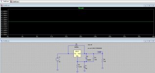
I have made schematic of how am I planing to wire the resistors (0R, 10R, 30R, 80R, 120R).
Is it okay if I make everything around the switch very neatly or should I add/make some kind of additional board?
Feeling very excited for testing phase ahead 😀.
Regards. Božo.

I have made schematic of how am I planing to wire the resistors (0R, 10R, 30R, 80R, 120R).
Is it okay if I make everything around the switch very neatly or should I add/make some kind of additional board?
Feeling very excited for testing phase ahead 😀.
Regards. Božo.
Last edited:
Is it okay if I make everything around the switch very neatly or should I add/make some kind of additional board?
Looks good! Putting the resistors right on the switch is the best way, if you can get them to fit. 🙂 Good choice of resistor values too. It will be fun to try that switch with headphones of different impedances and sensitivities!
Finally finished my ODA board and tested the voltages so far and something seems fishy, While the positive rail gives me 12.45V, negative rail gives me as low as 12.3V sometimes slowly climbing from 12.1V.
I have checked the IC's, capacitors and diodes - all properly oriented.
I have wired the rear RCA input to current buffered front RCA, JP1 to JP20.
Can I wire ODAC to JP21? Or should I use DPDT switch to cut off ODAC even when not powered on?

I am will also make better heatsink tomorrow scrapped from old PC PSU.
I have also shorted output resistors, I plan to install rotary output impedance switch later.
I have checked the IC's, capacitors and diodes - all properly oriented.
I have wired the rear RCA input to current buffered front RCA, JP1 to JP20.
Can I wire ODAC to JP21? Or should I use DPDT switch to cut off ODAC even when not powered on?
I am will also make better heatsink tomorrow scrapped from old PC PSU.
I have also shorted output resistors, I plan to install rotary output impedance switch later.
Your board looks great! 🙂
This is where those power disconnects, JP18 & JP19, really come in handy. I would suggest removing both of those jumpers to isolate the power supply section and see what voltage you get. Then try loading the power supply rails with resistors to ground from the "live" side of JP18 & JP19. Just something that would pull around 200mA - 300mA from the rail, like 50 ohms 5W. So 12.4/50 = 250mA, 0.25^2 * 50 = 3W. If your power rails stay stable with the loads, then the problem must be a short (or just an excessive load) out in the circuitry.
I'll take a guess that you may have either a bad LT voltage regulator or maybe a bad solder connection. The voltages on the power rails should be very stable if all is OK. Also - please take some close-up photos of your power supply section, top and bottom. Maybe I can spot something. 🙂
Unfortunately JP20 can't be run to JP1 because IC8 needs a resistor to ground on the input for input bias current return. JP20 has to connect to JP7, where it uses R16 and R17 for ground return. The outer two pins of JP20 go to JP7. JP7 is on the output of the input select switch, so whichever input you have selected (3.5mm front panel or RCA rear panel) will be sent to the IC8 input and out JP21 and the front RCA jack.
The ODAC output can't connect to JP21 because that is the output of IC8. The ODAC output can be connected to either JP1 (if you plan on not using the rear RCA input) or JP2 + JP3 (if you are not planning on using the front 3.5mm jack). So the input select switch then will select you ODAC as one of the choices, whichever jack you have it wired to.
Another completely different way to wire things here is leave IC8 unpopulated, then run JP1 to JP21. This just runs the rear RCA inputs directly to the front RCA output. Any load on that front RCA output will appear in parallel with the ODA's 10K input load on the rear RCA inputs. A couple of people who have built the ODA have just left the front RCA jacks unused, and I know of a couple of others who have run a pass-through like this from the rear to front RCA jacks. Then if you are not planning on using the front 3.5mm jack, connect the ODAC to JP2 + JP3. One input select switch position would then give you the rear RCA input, and the other the ODAC. If you do plan on using the front 3.5mm jack then you could connect an external DPDT between the ODAC output and JP2 + JP3, just like you said. That would isolate the ODAC outputs when the front 3.5mm jack is being used.
Please let me know if I can answer any questions on this wiring! 🙂 There are several different ways things can be wired with that pre-amp section and front panel RCA jack.
Finally finished my ODA board and tested the voltages so far and something seems fishy, While the positive rail gives me 12.45V, negative rail gives me as low as 12.3V sometimes slowly climbing from 12.1V.
This is where those power disconnects, JP18 & JP19, really come in handy. I would suggest removing both of those jumpers to isolate the power supply section and see what voltage you get. Then try loading the power supply rails with resistors to ground from the "live" side of JP18 & JP19. Just something that would pull around 200mA - 300mA from the rail, like 50 ohms 5W. So 12.4/50 = 250mA, 0.25^2 * 50 = 3W. If your power rails stay stable with the loads, then the problem must be a short (or just an excessive load) out in the circuitry.
I'll take a guess that you may have either a bad LT voltage regulator or maybe a bad solder connection. The voltages on the power rails should be very stable if all is OK. Also - please take some close-up photos of your power supply section, top and bottom. Maybe I can spot something. 🙂
I have wired the rear RCA input to current buffered front RCA, JP1 to JP20.
Can I wire ODAC to JP21? Or should I use DPDT switch to cut off ODAC even when not powered on?
Unfortunately JP20 can't be run to JP1 because IC8 needs a resistor to ground on the input for input bias current return. JP20 has to connect to JP7, where it uses R16 and R17 for ground return. The outer two pins of JP20 go to JP7. JP7 is on the output of the input select switch, so whichever input you have selected (3.5mm front panel or RCA rear panel) will be sent to the IC8 input and out JP21 and the front RCA jack.
The ODAC output can't connect to JP21 because that is the output of IC8. The ODAC output can be connected to either JP1 (if you plan on not using the rear RCA input) or JP2 + JP3 (if you are not planning on using the front 3.5mm jack). So the input select switch then will select you ODAC as one of the choices, whichever jack you have it wired to.
Another completely different way to wire things here is leave IC8 unpopulated, then run JP1 to JP21. This just runs the rear RCA inputs directly to the front RCA output. Any load on that front RCA output will appear in parallel with the ODA's 10K input load on the rear RCA inputs. A couple of people who have built the ODA have just left the front RCA jacks unused, and I know of a couple of others who have run a pass-through like this from the rear to front RCA jacks. Then if you are not planning on using the front 3.5mm jack, connect the ODAC to JP2 + JP3. One input select switch position would then give you the rear RCA input, and the other the ODAC. If you do plan on using the front 3.5mm jack then you could connect an external DPDT between the ODAC output and JP2 + JP3, just like you said. That would isolate the ODAC outputs when the front 3.5mm jack is being used.
Please let me know if I can answer any questions on this wiring! 🙂 There are several different ways things can be wired with that pre-amp section and front panel RCA jack.
Last edited:
Thanks Martin!
After some revision I think I might have found the source of my problems
I have reversed one of the rectifier diodes-D5 🙁it was hidden under IC) I immediately re soldered the diode(and tested the diode for forward and reverse bias and it was okay).
I also installed dummy load between JP18&JP19, 80R 10W(didn't have 50R). Resistor got warm and and rails were stable with negative rail still being at higher voltage(because it is negative).
With power disconnected at JP18&JP19 I measured +12.483V and - 12.402V.
That seemd okay so I thought I should power up everything. Amp did work, 3,5mm was used as input input and right channel was louder and cracking/popping cracking/popping could be heard, when the pot is moved it cracking gets more pronounced. With music playing that few seconds positive rail was at +12.470V and negative was at -12.394V.
As for the pre Amp wiring. When JP20 to JP7 are connected, which one is left and which one is right on JP7 in respect to JP20?
I would like to use all options with IC8, but I can also ditch the chip if necessary -3.5 mm input, rear RCA, DPDT-ed ODAC all with front RCA otuput.
Also does it matter if the IC8 adds some DC offset to ODAC's otput?
With IC8 I used R90, R52, R56 and C41 and C43.
Here is a link to Gdrive folder with photos.
https://drive.google.com/drive/folders/0B40kmOKTFDu0ZTVLSDZzSGZiN28
Regards, Božo.
After some revision I think I might have found the source of my problems
Great work on tracking that rectifier down! Your 80R load is just fine. Your measured rail voltages look great too.
Interesting about the noise with the pot being turned! Hmm... that shouldn't be happening. Thanks for those high resolution pictures too. It is midnight here right now - I'll read through in more detail tomorrow and give you some answers. 🙂
After some revision I think I might have found the source of my problems
I have reversed one of the rectifier diodes-D5 🙁it was hidden under IC) I immediately re soldered the diode(and tested the diode for forward and reverse bias and it was okay).
I also installed dummy load between JP18&JP19, 80R 10W(didn't have 50R). Resistor got warm and and rails were stable with negative rail still being at higher voltage(because it is negative).
With power disconnected at JP18&JP19 I measured +12.483V and - 12.402V.
OK I'm back the computer! 🙂 So here is some interesting things about your power supply measurements.
I wasn't sure exactly what revsersing D5 would do, so I simulated it, results below. Turns out it essentially bypasses the pre-regulator and lets nearly the full input voltage go to the LT3015. In this sim I have 24Vdc going into the LM317 and 1.6V less, 22.4Vdc comes out. That 24Vdc input would be the result of a 18Vac transformer secondary.
So - you are lucky this happened with the negative power rail because the maximum input voltage of the LT3015 is 30V, but for the LT1963A on the positive rail it is only 20V. That is one of the reasons I have the pre-regulators on there, to drop the input voltage down enough for the LT1963A chip. If your input voltage (JP11) isn't running more than 30V, your LT3015 should be OK, at least no over-voltage. But the LT3015 would wind up with 12V across it and it would get hot fast, since it doesn't have a heat sink. The LT3015 has thermal shutdown though, so it probably survived the dissipation if it didn't run very long that way.
Long story short: your LT3015 probably survived. 🙂
The regulator chips all have a certain amount of natural +/- tolerance on their internal "set" voltages, which is what causes the small amount of variation from the +/-12.5Vdc power rail target voltage. In your case the 12.483Vdc positive rail came out great, but the internal reference votlage of that LT3015 is off a tiny amount to result in -12.402Vdc. Here is where it gets fun though. 😀 Even though the 0.08Vdc difference really doesn't matter, it would jsut reduce the maximum output swing by that amount, why not get it perfect? That is why I put the two "set" resistors in series on each regulator, R35 and R36. That 60.4 ohm R36 can be changed to get the two voltage exactly matching.
Starting with your measured -12.402 I worked the voltage set equation under figure 2 in the LT3015 datasheet backward to come up with what the actual internal reference voltage in that chip is running at, -1.2115Vdc rather than the "typical" datasheet value of -1.22Vdc. Then using that equation with the calculated -1.2115 set voltage to produce -12.483Vdc output, to match your positive rail, comes up with using a 48.2 ohm resistor instead of the 60.4. The closest standard value is 48.7 ohms, which should produce -12.480Vdc. I just happen to have some 48.7 ohm resistors here, I'll put one in an envelope for you, no charge. 😀
I'll make a seperate post with the rest of your question. 🙂
Attachments
Last edited:
That seemd okay so I thought I should power up everything. Amp did work, 3,5mm was used as input input and right channel was louder and cracking/popping cracking/popping could be heard, when the pot is moved it cracking gets more pronounced. With music playing that few seconds positive rail was at +12.470V and negative was at -12.394V.
Hmm... still thinking about this one. It would be worth re-heating the solder joints on both the volume pot and the gain switch. From the photos it looks like you used the Bourns pot. If you had used Alps I would have said that is likely the problem, I have had several Alps pots bad right out of the package, brand new. So far I haven't had any bad Bourns pots.
I'll ponder this tonight and see if I can come up with some ideas on tracking the problem down.
As for the pre Amp wiring. When JP20 to JP7 are connected, which one is left and which one is right on JP7 in respect to JP20?
Pin 2 of JP7 is left, which is the hole closet to the board edge & 3.5mm input jack. Pin 3 of JP20 is left, which is the one closest to the IC8 chip. From your photos it looks like your red/black wire is left and may need to be swapped on one end with the right wire. Hey those are *excellent* high resolution photos! I can zoom way in on them and see detail. 🙂
I would like to use all options with IC8, but I can also ditch the chip if necessary -3.5 mm input, rear RCA, DPDT-ed ODAC all with front RCA otuput.
Sounds good, it would be best to add an external DPDT switch then (actually DPST, but just use half) between your ODAC output and the JP2 + JP3 input pins, so you can switch the ODAC output out of the circuit if you need to use the 3.5mm jack.
Also does it matter if the IC8 adds some DC offset to ODAC's otput?
With IC8 I used R90, R52, R56 and C41 and C43.
The addiional input bias current from IC8 through R16 and R17 may very well add (or subtract, depending on the polarity of that IC8 input bias current) a mV or two of DC output offset from the gain stage of the ODA, *but* that stage is capacitor coupled to the output stage, just as in NwAvGuy's O2 headamp, so it won't matter. None of the output offset from the gain stage - or any DC on the input from the source! - makes it through to the output stage.
Your IC8 part values would give you 1x voltage gain, just a current buffer, which is a good place to start. If you find you need some votlage gain for yoru pre-amp outs in the future you can add R49 and R55. Votlage gain = (1 + R56/R55) and same for the other channel. You will also need to install R57 and R62 to connect the output of IC8 to the RCA jacks. The purpose of those 20R resistors is just to isolate the RCA cable capacitance. The input Z of speaker amplifiers is usually a large 10K - 50K, so that output resistance shouldn't matter to the signal.
That was so informative!
Huh, I am very lucky indeed to turn D5, lol.
I hope LT3015 survived. It did not work like that for a long time, hopefully it's lifespan does not shorten or it's parameters got messed messed up.
Nothing on board ever got hot or smoked. Even without heat sinks IC6 and IC7 are just warm to touch(they do not dissipate that much heat without the case, my workplace is not very warm though).
I do like your "get it perfect" approach. I think it makes up for a great amplifier circuit.
Thank you for the resistor, I appreciate it 🙂.
I have finally gotten some time to play with amplifier(fixing those input to IC8 wires adding R57, R62 and one gain resistor on one channel that caused imbalance on gain switch position 2. Also added D7 to AC jack.
Took more measurements while amp was working(no input)
Here are some measurements with amp working without the load.
JP 16: +14.660V
JP 17: -14.281V
JP 8: +24.660V
Jp 9: -24.530V
My subjective impression is that IC6 might be running lightly warmer than IC7. Did not measure the temperature, so this is not reliable info.
Now. This is very interesting.
Measuring DC offset on L and R I have found that both of them were significant and were causing that loud cracking sound(pronounced in R channel). Offset itself was pretty big around - 0.3mV and - 0.5mV.
Trim pots were adjusted before installation but still there was pretty big offset.
I took the leads of multi meter, shorted them somewhere on board and and took relative measurement of 0.00mV.
Left trimpot had to be turned quite a few times(five or so) counterclockwise to get 0.00mV. Turning the right one in same direction I hit the limit of the trimpot resulting in -0.33mV.
Both oscillate from time to time, left one +- 0.001mV, right one -0.33mV to -0.4mV(yes, minus voltage).
With that all the cracking/popping was gone completely and the amp sounds great.
I rechecked all the DC offset zeroing circuit components and all where in place.
Wondering what would be the cause of that DC offset?
bozoc - your power supply measurents look good. You are right, there is only a volt or so across those LT LDO regulators, so very little heat generated. The pre-regulators burn off most of the voltage drop.
Interesting about the DC offset! Your left channel results sound OK. The trimpots are 25 turn, 12 each way from center, so 5 turns is still in the normal range. Tolerances in the zener diode and offset differences in the NJM4556A chips. That 1uV of drift is good - once the amp is boxed up (in the standard B4 case anyway) +/-20uV of thermal drift in DC output on each channel is pretty common. Your right channel does sound like there is a problem. My first guess would be one of the NJM45556A chips may be bad and has significantly more offset that the others. I tested a large number of the NJM4556A chips during the design phase and they all had offsets of the same polarity and grouped fairly close together.
Let me see if I can come up with a way to track it down. Would you have access to a vacuum desolderer to get those SIP NJM4556A chips out on that channel? If it does turn out to be a bad chip the easiest way to test is plug them into a solderless breadboard wired up as two unity gain buffers, with the inputs grounded, and test each chip's actual DC offset.
Before you pull them though lets do a few more voltage checks to make sure the problem isn't in the DC offset null circuit.
Last edited:
I do have access to de soldering vacuum pump.
ICs that buffer current for the right side are IC10, IC13 and IC15?
Checking the components of DC zeroing circuit showed that they are all in place. Only thing that could be faulty I guess are the Zeners.
Measuring forward bias in them sowed 0.7295V for D14 and 0.7313 for D11V.
Voltage drop on D14 was 2.514V and 2.505V while the amp was on.
This time right channel was pretty wild, with big oscillations, oscillating for 1mV at the moments!
Left channel was solid still at -0.002mV(this time it was colder).
I will try re soldering components around right channel ICs, but I doubt it will help.
If there is no other option I will de solder those and test them.
bozoc - that is correct, IC10, 13 and 15 for the right channel.
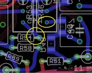
Good that you measured the zener voltages, those look OK. Also see what you get across the trimpots at the measurement points in the image below. Each zener feeds a trimpot through a voltage divider. That circled end of R54 would let you measure the left trimipot, but for the other you may need to solder a small wire to the trimpot lead under the board to measure it.
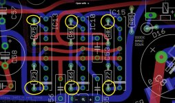
The other image is an idea for trying to track down which output chip might be bad. try measuring the voltages to ground at the points in the yellow circles. Those are just the points where the output of each chip section feeds a balancing resistor. If one chip or chip half has an excessive offset it may show up there.
Also, I wanted to check that your headphone relay circuit is working OK. Do you get the 3-second or so delay between when you turn on the power and when sound comes out?
Good that you measured the zener voltages, those look OK. Also see what you get across the trimpots at the measurement points in the image below. Each zener feeds a trimpot through a voltage divider. That circled end of R54 would let you measure the left trimipot, but for the other you may need to solder a small wire to the trimpot lead under the board to measure it.
The other image is an idea for trying to track down which output chip might be bad. try measuring the voltages to ground at the points in the yellow circles. Those are just the points where the output of each chip section feeds a balancing resistor. If one chip or chip half has an excessive offset it may show up there.
Also, I wanted to check that your headphone relay circuit is working OK. Do you get the 3-second or so delay between when you turn on the power and when sound comes out?
Attachments

Last edited:
bozoc - Another observation (ran out of edit time on the post above), the polarity of the offset on the right channel is negative, which probably indicates a bad chip. The NJM2068 usually have a positive offset, which is why the offset zeroing circuit is fed from the negative rail and produces a negative voltage to zero out the chip's positive offset. It could be that one of the chips on the right channel has a negative offset which is adding to the zeroing circuit output rather than cancelling. Hopefully measuring the chip output voltages feeding the 1R resistors in that image above will track down which chip. I have a bunch of those NJM2069 SIP chips here, I can send you chip(s) along with the resistor. 🙂 In the meantime if you can track down which chip, just remove it and run with only the other two. So two NJM4556A in parallel on that channel rather than 3. That is assuming it is only one chip that is bad, of course.
Last edited:
It takes about 4 sec for the relay to kick in and to produce sound.
Voltage drop on trim R64 is -2.95mV and on R53 -3.05mV.
Other measurements I took are interesting.
When I turned on the amp voltage on the right side(points marked on photo) were going crazy, moving from -100mV to -10mV, while the right side was stable.
Voltages on left side were fairly stable around -0.4mV.
As the amp was on for a few minutes voltages on the left side of current buffers stabilized even further sometimes giving even +0.3mV but usually settling around -0.2mV.
Crazy right side was still oscillating around -10mV mostly from -9mV to 15mV.
All the voltages all ICs are quite similar if not the same with some exceptions. From time to time I would get positive offset on IC15 around +10mV. I would also get +0.2mV on IC14.
agdr - How often do NJM2068 have negative DC offset?
I think it is quite interesting that there is so much negative DC offset in the batch I got.
Or. . . Something is wrong with the circuit.
This line in previous post.
Crazy right side was still oscillating around -10mV mostly from -9mV to 15mV.
It is -15mV.
I think it is quite interesting that there is so much negative DC offset in the batch I got.
Or. . . Something is wrong with the circuit.
This line in previous post.
Crazy right side was still oscillating around -10mV mostly from -9mV to 15mV.
It is -15mV.
It takes about 4 sec for the relay to kick in and to produce sound.
Voltage drop on trim R64 is -2.95mV and on R53 -3.05mV.
Changing C50 to 3.3uF from the 4.7 will reduce that relay delay to about 3 seconds. In the Super CMOY project I've decided that 4 seconds is a bit too long to wait for a headphone relay to close, 3 is better. I'll send you a 3.3uF with the resistor and you can change it if you want. 🙂 I've also just posted a ODA BOM revision with that one change for C50 out on the Google Drive link. Also attached below as a zip.
Your trimpot measurements look great. The average offset of the NJM4556AL chip is around 1.5mV, so I set the trimpots up with twice that across them to give around 1.5mV at the pot center.
I have an idea. 🙂 The 1R balancing resistors are small enough that they are forcing all the outputs to measure about the same. To find the bad chip the outputs need to be isolated. It will be a lot easier to lift one end of resistors rather than remove the NJM4556ALs. so one thing to try is unsolder and lift out the 6 circled 1R resistor ends below. Then measure the voltage on the empty PCB pad, which will be the output of each half-chip. Then the culprit should show up.
In fact for starters, maybe just lift that one end of the top 3, R75, R68, and R81. That would give you half of each of the 3 right channel chips. The thinking here is if a chip is bad, both halves may be bad. If you can use the vacuum desolder those 3 resistor leads should come right out. Otherwise I usually just stick my soldering iron tip under the lead at the end of the resistor, heat it up and pry it out. Then clean out the hole with solder wick or taping the board lightly while the pad is hot.
It will be really interesting to see the DC offsets of the 3 chip halves with those balancing resistors disconnected! They should be 1.5mV +/- 0.3mV or so. When you make the measurements probably best to have any input sources unplugged and the input select switch set for the front panel 3.5mm jack, since it grounds the inputs with nothing plugged in.
If those 3 chip half outputs look normal then go ahead and unsolder the ends on the other 3, R73, R66, R77 and then take those chip output measurements for the other chip-halves.
We should be able to track it down to just the one chip that is bad and needs to come out! 🙂
agdr - How often do NJM2068 have negative DC offset?
Not very often. I tested a pile of 40 chips at the start of the project, bought at different times in 3 different batches and the output offset of them all were around +1.5mV, +/-0.3mV as I recall. There is a post earlier in the thread with the statistics from a test of a group. Most likely it is just one chip that is bad, but with the small 1R balancing resistors it is dragging the other two outputs along with it.
Attachments
Last edited:
agdr- I have desoldered all balancing resistor connections at the points on the diagram.
They still crazy oscillate sometimes to -100mV when after the amp was just turned on.
Sometimes voltage settles to around -10mV.
I think it is the best if I desolder them all and test them.
If I have small negative offset in my left channel too, does that mean that there might be bad chip in left channel too?
Unrelated.
I find this idea pretty nice regarding the front panel design.
https://www.youtube.com/watch?v=Yj0Bv4UEFSs
agdr- I have desoldered all balancing resistor connections at the points on the diagram.
They still crazy oscillate sometimes to -100mV when after the amp was just turned on.
Sometimes voltage settles to around -10mV.
I think it is the best if I desolder them all and test them.
If I have small negative offset in my left channel too, does that mean that there might be bad chip in left channel too?
Unrelated.
I find this idea pretty nice regarding the front panel design.
https://www.youtube.com/watch?v=Yj0Bv4UEFSs
Thanks for the front panel link!
Please tell me a little more about the right channel. I want to confirm my understanding that you unsoldered all six 1-ohm resistor ends, and when you measure the pad the resistor used to go through you get 10mV on all 6 pads (no longer touching the resistor lead that has been removed on each of course)? Also would you post a picture in your gallery of the way the board is right now with all 6 resistor ends unsoldered? As they say here, a picture is worth 1000 words. 🙂
If so that is definitely not correct. There should be around 1.5mV on all 6 op amp outputs. With those resistor ends unsoldered the NJM4556A's are not tied together at the outputs in parallel anymore and each one should be able to settle at its own offset level. 10mV on any of them is way out of the ball park. The good news here is with it that far off the problem will be easier to find!
One thought I have, 10mV of offset is bad enough that it would indicate either a bad chip or damage, and if more than one NJM4556A (all 3 in this case) are doing it that would have to be damage. Thinking back to the power supply issue you were having, I'm wondering if the full -24V made it out to the circuitry somehow. With D5 reversed we figured out that the full -24V went to the LT3015, but it should have survived, athough it probably went into thermal shutdown from time to time. A thought just occurred to me. I've been assuming that when the LT3015 goes into thermal shutdown the output turns off, but maybe instead it "drops out" and lets the input voltage go straight to the output. That would have sent bursts of -24V out to the circuitry every time it went into shutdown. I'll study the datasheet and see if I can figure out what it does in thermal shutdown. The NJM4556a chips may not handle over-voltage as well as the newer LME49990 chips. But still it is interesting that only the right channel seems to be affected.
Now on the left channel I want to make sure I understand the amount of offset you are measuring there. It sounds like it is around 1 microvolt (= 0.001 millivolts, of course), or do I have that wrong? 1 microvolt would be considered fantastic for the ODA if it is stable. Typically you will get +/-20 microvolts of thermal drift as the chips warm up and/or when it is boxed up. But 20 microvolts shouldn't be enough to make an audible thump or click in any headphone or IEM, even if 115dB/V sensitivity. So if the left channel is producing a thump with just 20 microvolts DC offset there may be another problem. By way of comparison the typical DC output offset on NwAvGuy's O2 Headphone Amplifier is 3.3mV = 3300 microvolts! And he considered that OK. 🙂 At 20 microvolts that would be just 0.6% of the O2's DC offset.
Which reminds me, please tell me again which headphone or IEM (impedance and sensitivity) you are using for your testing.
We will get it all figured out! 🙂
And very happy holidays to you and your family!!

Last edited:
Please tell me a little more about the right channel. I want to confirm my understanding that you unsoldered all six 1-ohm resistor ends, and when you measure the pad the resistor used to go through you get 10mV on all 6 pads (no longer touching the resistor lead that has been removed on each of course)?
I added two photos(named them accordingly) to my ODA Gdrive album, I have also damaged C46 while desoldering R81 🙁, I will replace that cap although it measures fine.
https://drive.google.com/drive/folders/0B40kmOKTFDu0ZTVLSDZzSGZiN28
I have also took new measurements on empty pads. It is interesting how voltage changes with time. When the amp is turned on, left side is crazy high, up to -100mV and sometimes even positive 100mV(mili - m, not micro - μ; that is as low my multi meter can go, although it can detect change that low, precision is not so good). If the the amp is working for few minutes it goes down to -20mV or so on the right side.
Left side is around +-0.02mV.
All the measurements are taken with 3.5mm input selected, without input signal, volume on max, gain on first position with right side resistors unsoldered like in the diagram you linked unless noted otherwise.
https://drive.google.com/drive/folders/0B40kmOKTFDu0VUtLY0d4MzRCQWM?usp=sharing
I am using throwaway headphones similar to these, they share the same driver I am sure of that.
https://www.sharkoon.com/product//15894#desc
32 Ohms and sensitivity of 102 dB ± 3 dB.
Thank you very much 🙂.
Happy holidays to you and your loved ones!

bozoc - thank you for the pictures and information!
I'll bet I have 300+ of those little blue caps here. 🙂 I'll put some in the package. 🙂
I've thought of two more things to take a look at. If you have access to a scope it would be a good idea to take a look at both power supply rails, especially that negative rail. If the LT3015 went bad it is possible there is ripple on top of the DC there. That would also account for the slightly different DC voltage. If no scope just the multimeter on AC might detect any ripple.
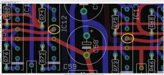
Another thing to measure is the input DC voltage going to both the left and right channels. I've circled the test points below in yellow. They are on the bottom of the board, you may want to temporarily solder a small wire onto those to bring it out where you can get a meter on it. These voltages are a mix what comes out of the DC zeroing trimpot wiper, minus the chip's input bias current voltage drop across the ground return resistor. There are some PCB via holes involved in getting the signal to the NJM4556A chips. Just want to make sure what is going into the NJM4556A chips looks good.
I'm going to send you a PM to right now with some thoughts. 🙂
I'll bet I have 300+ of those little blue caps here. 🙂 I'll put some in the package. 🙂
I've thought of two more things to take a look at. If you have access to a scope it would be a good idea to take a look at both power supply rails, especially that negative rail. If the LT3015 went bad it is possible there is ripple on top of the DC there. That would also account for the slightly different DC voltage. If no scope just the multimeter on AC might detect any ripple.
Another thing to measure is the input DC voltage going to both the left and right channels. I've circled the test points below in yellow. They are on the bottom of the board, you may want to temporarily solder a small wire onto those to bring it out where you can get a meter on it. These voltages are a mix what comes out of the DC zeroing trimpot wiper, minus the chip's input bias current voltage drop across the ground return resistor. There are some PCB via holes involved in getting the signal to the NJM4556A chips. Just want to make sure what is going into the NJM4556A chips looks good.
I'm going to send you a PM to right now with some thoughts. 🙂
Attachments
- Home
- Amplifiers
- Headphone Systems
- A version of an O2 Desktop Amp (ODA)