Been having bad weather here so some of my parts got delayed in shipping but finally able to start soldering today.
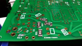
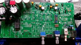
I attached a jpg of the 1st 5 resisters as per instructions. Other than the smaller one (R13) where I got a little too much solder on it, how's it looking?
Since this is my first attempt at SMD, wanted to get some feedback before getting far into the build. Any help/comment welcomed... too much solder, too little, looks like crap... etc 😀
I already dropped one of these little bastards and had a fun time finding it on the floor... lol.
Attachments
Other than the smaller one (R13) where I got a little too much solder on it, how's it looking?
Looks great!! In fact, as per R13, on the booster board as of late I actually have been going back and *adding* more solder to the ends after my first round so they wind up looking just like that. "flooding" the ends a little bit won't hurt, as far as I know, but I figure it ups the odds of missing a "dry" joint and flowing solder between the part and PCB pad.
I already dropped one of these little bastards and had a fun time finding it on the floor... lol.
Yep! 🙂 It is a really good idea to buy one additional of all the cheap(er) smd parts just in case one goes flying off the tweezers onto the rug, the cat, or places unknown like that. I've had it happen quite a few times.
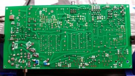
In looking at your photo I see two of the labelling errors with this last crop of boards. I have this in the build instructions, but just a reminder D17 does not go on those two pads. They stay blank. D17 is now leaded and solders directly across the AC power jack leads. Those D17 pads happened when I screwed up and specified a unidirectional SMD transorb rather than a bidirectional. The bidirectional is larger.
Then that rectangular box to the right of R21 with no text in it is a case of me getting the text on the wrong side of the board. Flip the board over and you will see the text that should have gone in the box. Those 4 marked rectangles are optional external (leaded) COG MLCC caps that solder across the electrolytic leads. The MLCCs are small and light, so probably best to first solder the electrolytics down. Then go back and reheat the solder on one lead and stick in one of the MLCC leads. Then repeat on the other electro lead.
Last edited:
Hey 4x4F150!
Congrats on starting your ODA build!! Your soldering looks great!
Please keep posting your progress...I found the entire build process of the ODA really a good experience and when you turn it on for the first time its a great feeling!
Congrats on starting your ODA build!! Your soldering looks great!
Please keep posting your progress...I found the entire build process of the ODA really a good experience and when you turn it on for the first time its a great feeling!
Congrats on starting your ODA build!! Your soldering looks great!
Please keep posting your progress...
Thanks! And here's the update:
Just finished step 1, but in my infinite wisdom... forgot to buy the ac adaptor 🙁 so testing is going to have to wait till it comes in this weekend. I refuse to continue to step 2 until step 1 tests well. Maybe have step 2 done this weekend as well...?
Some equipment tips for anyone out there going to do this build:
If your looking for an alternative to the panavise, this is a great cheap alternative: Aven 17010 Adjustable Circuit Board Holder. Off amazon, its only $13 😀 You can see it holding the board in the pics. Not nearly as adjustable or high quality as the panavise, but still got the good ol rotisserie action.
Also loving my new soldering iron from circuit specialists (NwAvGuy recommended them on his blog). Got the 75 watt yellow one for ~ $50 shipped off ebay (they have a store on ebay which is cheaper than directly from their website 😕).
Attachments
If your looking for an alternative to the panavise, this is a great cheap alternative: Aven 17010 Adjustable Circuit Board Holder. Off amazon, its only $13 😀
That is a fantstic find! I didn't know those existed. 198mm jaws, more than enough for the ODA aboard sideways.
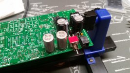
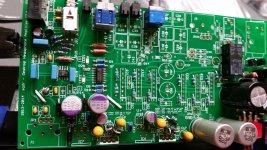
Everything looks good on your board so far. The main way anything can get messed up at this point is getting the polarity wrong on a diode or electrolytic capacitor. Always good to triple check those! I check them vs. the layout diagram (or Part ID diagram) since the polarity symbols on a lot of parts get covered up once they are installed.
You even soldered the two 0805 sized caps in just fine between the electrolytic leads on the bottom! I put those two rectangular markings (for the 0.1uF 50V) there in case anyone didn't feel comfortable with the 0805. They could just solder on two leaded caps, as with those other two electrolytics. I didn't put 0805 cap pads between the leads on the other two (the 820uF) because the electro lead spacing wasn't wide enough.
The usual advice on bypassing an electrolytic with a smaller value ceramic is to keep the leads as short as possible, so lead inductance doesn't block the higher frequencies you are trying to bypass. Well lead/trace length doesn't get much shorter than an 0805 sized COG cap right between the electrolytic leads.
Last edited:
Well lead/trace length doesn't get much shorter than an 0805 sized COG cap right between the electrolytic leads.
That's for sure 🙂
I didn't trim the length of the larger ceramic capacitors at all. Just wrapped them around the leads from the electrolytic caps from on the top of the board, solder them together, and trimmed the long leads from the electrolytic caps. I see now that the instructions do say to trim them solder, but I did the opposite and there wasn't anything to trim on the ceramic because of the solder. Should I de-solder the ceramic, trim the leads down to only what is needed, and re-solder? Or maybe I'm obsessing?
(Guess i was "in the zone" with the solder, trim, repeat pattern)
4x4F150 - they way you did the ceramic cap leads by wrapping them around the electro and then soldering is perfectly fine. In fact, that will be the most mechanically stable. I do mine that way. I just have it the other way around in the build instructions to make the build a bit easier by keeping the electrolytics soldered down firm on one lead while working on the other. The ceramics are so light the solder alone is more than enough to hold them. But either way is just fine electrically.
Hey on the power transformer, it is sort of a chunk and can take up a lot of outlet or power strip space. I highly recommend these 8" power strip break-out cords at Walmart:
http://www.walmart.com/ip/Woods-8-16-3-SPT-2-Adapter-Cord-White-3pk/16489603
It says out of stock but last I looked every walmart in the area has them. They work great! The transformer only takes up one outlet space.
Last edited:
Hey on the power transformer, it is sort of a chunk and can take up a lot of outlet or power strip space
That's an understatement... Holy hell, this thing is huge! 😱
By far the largest wall wart I've ever owned. No worries though, it's going to be plugged into a large APC UPS, so I have tons of room.
That's an understatement... Holy hell, this thing is huge! 😱
Lol! When it comes to power supplies the ODA doesn't mess around. 😀
An externally hosted image should be here but it was not working when we last tested it.
Build update:
Tested step one and everything was within 0.1 V 😀
Just finished step 2 and 3 and board photos below. (Step 3 is pretty short)
I did have a minor heart attack after completing step 2 where the directions started listing a few measurement for some jump points and mine were all 0V. Went back and read the whole paragraph for voltage listings and the last sentence says "Voltage testing in this section will be done at the very end of this build". Don't do that to me!!! Put that as the first sentence lol. I should have paid more attention to the previous paragraph that explains why this section of the board doesn't have power yet.
Also had trouble with my DMM. It was reading the output of the transformer as only 0.3V. I then checked the DMM by measuring the output of a wall outlet and it only measure 0.58V 😕 Went and bought another DMM and the wall outlet measured 120V like it should and everything on the board measured well. I've never seen a DMM do this, they either work or don't (and this was on fresh batteries too). Threw that thing into the trash.
And I just have to say... building this thing is so much fun. It's like an adult lego set 🙂
Attachments

Last edited:
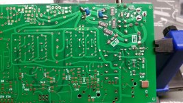
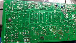
4x4F150 - nice job! 🙂 Good thoughts about moving that notice about the power supply being checked later right at the front of the section. I'll do it. 🙂 Your soldering job on the TL064 leads looks just excellent.
Those long jumpers from the CRC filter section to the regulator section are a result of the horizontal layout along the back panel for heatsinking. Everything lays out very well except the interconnection between the two sections. Rather than place the power feed into the regulators, which has the AC sawtooth wave on it, as traces right over the "clean" DC output traces on the PC board I just went with two jumper wires. Problem solved!
That is odd about the DMM. They have a fuse on the current measurement test lead socket that gets blown but it shouldn't effect the AC volts testing. Yep, that meter goes in the trash!
Last edited:
4x4F150 - nice job! 🙂
Thanks!
And another update - step 4 done with pics below.
This step was pretty straight forward, but wow are R1 and R2 tiny. Had little problem with getting those 2 in with no solder bridge to the input jack right next to them. I don't think it really would matter cause I'm pretty sure they are connected in the board. But everything is looking good now. 🙂
Hope to have time to do step 5 tomorrow. Till then, cheers!
Attachments
Finished step 5.
But found my first mistake... I put resistor fifty on the spot for resistor fifteen (they sound too similar 😀). You can see it in the pics below (took the pics before I noticed the problem). When I removed R50 from the wrong spot, one side kind of "ripped off". What I mean by this is that before you solder them in, the SMD sides are silver. After pulling R50, one side was mostly white like the bottom. I checked R50 with my DMM and it still measures 1k ohm, so I soldered it into the correct location and measured again... still 1K ohm.
I assume this will be OK since it still measures the correct value...?
Also have question about the preamp section which is coming up soon. I want to control the volume of my powered monitors with the ODA (which will be connected to the pre-amp out of the ODA). I'm pretty sure that fmcclell wanted a similar thing but also want to cut the sound going to the pre-amp. From what I read in agdr reply is to take the holes of R89 and R88 to JP21 holes 1 and 3. But should it be R89 -> JP21 hole 1 and R88 -> JP21 hole 3 or the other way around?
I am guessing the way I listed because R89 goes to JP22 hole 1 and R88 goes to JP22 hole 3 (both through the relay). And what about hole 2... jumper those together or no?
I don't want to flip-flop the left and right channels on the pre-amp. I will also be removing R62 and R57 to "cut out" the preamp chip.
Attachments
Last edited:
Finished step 5.
But found my first mistake... I put resistor fifty on the spot for resistor fifteen (they sound too similar 😀).
I actually spotted that this morning looking at your photo, but had to run out and didn't get a chance to post until now. 🙂 Those resistos are the same deal as post #716 and #717 above with Turbon's build.
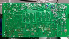
Your build is coming along very nicely! Your high rez photos are excellent. They will help other folks. For anyone else viewing these, remember that clicking on the four arrows in the bottom left of the photo will expand it even larger (then use the scroll bars that show up).
I see you installed the two attenuation resistors, R31 and R32. If you should decide not to use those at some point I would recommend just leaving them installed, but jumpering them over on the bottom of the board. That leaves to the option to use them open for the future. The attenuation resistors cut the maximum output swing in half, but give you a 1/2x (attentuation) first position on the gain switch. So - which is the case with me - if you headphones all need 3.5Vrms or less but some of your sources put out more than 2V, the attenuation resistors are just the ticket. But if you have headphones that need more than 3.5Vrms swing you can't use the atten resistors.
Another way to get 50% attenuation is just increase the two input resistors from 274R to 10K, but that will add a tiny amount of Johnson noise to the input.
Yeah luckily on R1 and R2 they are just jumper resistors. If anyone doesn't want to muck around with 0603 sized soldering just tin the two pads, tin the end of a small wire, and then solder it on. Clip off the excess. Problem solved! 🙂 Those jumper resistors are the equivalent of halving to cut the two traces under the input jack on the O2 to use the external input pins. Here no traces to cut, just leave R1 and R2 off.
Your R50 should be OK since it still measurea OK. But I'll drop one in the mail for you tomorrow just to keep on hand. R50 doesn't do anything most of the time anyway. 🙂 That is a "safety" resistor to insure a path to ground for the output chip's input bias current if, years down the road, the DC zero trimmer pot develops a loose wiper. I did reliability and maintainability engineering on fighter jet electronics in college one summer at a defense contractor, then years later was at a process controls company where reliability is everything (chemcial plants, etc. that can blow up if the control systems ever go down) so I've wound up as kind of a high-reliability design nut. I'm always thinking about what will happen given overvoltage, voltage dropout, hot & cold, vibration, EMI, component failure, component drift, magnetic fiields, you name it. 😱 Lol - NwAvGuy got frustrated with some of my O2 amp reliability suggestions once and PMed something like "its not going into space!".
A tip on removing the SMD resistors is take a piece of copper solder wick braid, place on top or to the side of the part, and heat it up. The braid will transfer heat to both ends and melt them. Also just heating one end long enough will usually eventually loosen the other. But that might also life the PC board trace - the solder wick is the safe(r) way.
On the pre-amp out, do you plan on using the headphones and speakers at the same time, or one or the other? In fmcclell's case he wanted to use one or the other, and his headphones luckily didn't need more than roughly line-level types of voltages, so the solution was just run the output of the ODA to a (front panel DPDT) switch that would switch the output to ether the front panel 1/4" jack for his phones, OR the pre-amp for his output. He wanted one cut off like that when the other was in use.
Last edited:
On the pre-amp out, do you plan on using the headphones and speakers at the same time, or one or the other?
Only one will be used at a time, but I already sent off my front and back panels so I won't have a place for the switch in the front panel to toggle the two. Not a big deal, I'll just plug in headphones when I use them. I see a lot of headphone amps where the volume knob controls both the preamp out and the headphone volume, and that's what I was aiming for here. The powered monitors have their own amp, just need to control the volume.
And I'll let you know if this thing ever makes it to space... lol 😀
Last edited:
4x4F150 - with one of these you could make a really nice panel hole just with a hand drill if you wanted:
Titanium Nitride Coated Steel Step Drill Bit Set
It wouldn't have the D hole shape, but a bit of epoxy on one side would keep it from rotating.
Titanium Nitride Coated Steel Step Drill Bit Set
It wouldn't have the D hole shape, but a bit of epoxy on one side would keep it from rotating.
Agdr - But should it be R89 -> JP21 hole 1 and R88 -> JP21 hole 3 or the other way around? And leave JP21 hole 2 alone?
All above is assuming I understood what fmcclell was trying to do is the same thing that I am trying to do with the preamp out. Except no switch.
All above is assuming I understood what fmcclell was trying to do is the same thing that I am trying to do with the preamp out. Except no switch.
Agdr - But should it be R89 -> JP21 hole 1 and R88 -> JP21 hole 3 or the other way around? And leave JP21 hole 2 alone?
It should wire as R89 -> JP21 hole 3, R88 -> JP21 hole 1, and then you need to install R90, which is a jumper to ground which will ground JP21 pin 2. I'll put a jumper 1206 resistor in the envelope on Monday too.
If you don't use a switch you will still need jumpers in the R88 and R89 positions to connect the amp output to the 3.5mm and 1/4" output jacks. Just solder those wires going to JP21 right onto the jumper wires. So your pre-amp outs will just wind up in parallel with your two output jacks.
Last edited:
- Home
- Amplifiers
- Headphone Systems
- A version of an O2 Desktop Amp (ODA)